

Etching agent for copper or copper alloy
a technology of etching agent and copper alloy, which is applied in the manufacture of cable/conductor, basic electric elements, chemistry apparatus and processes, etc., can solve the problems of sensor malfunction, bump deformation, and miniaturization technology approaching its limits, and achieves high selectivity
Active Publication Date: 2014-08-28
SAMSUNG ELECTRONICS CO LTD
View PDF7 Cites 14 Cited by
- Summary
- Abstract
- Description
- Claims
- Application Information
AI Technical Summary
Benefits of technology
The invention provides an etching solution that produces less foam and can selectively etch copper or copper alloy in electronic substrates containing both copper and nickel.
Problems solved by technology
However, particularly in semiconductor devices, the miniaturization technology is approaching its limits.
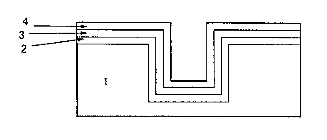
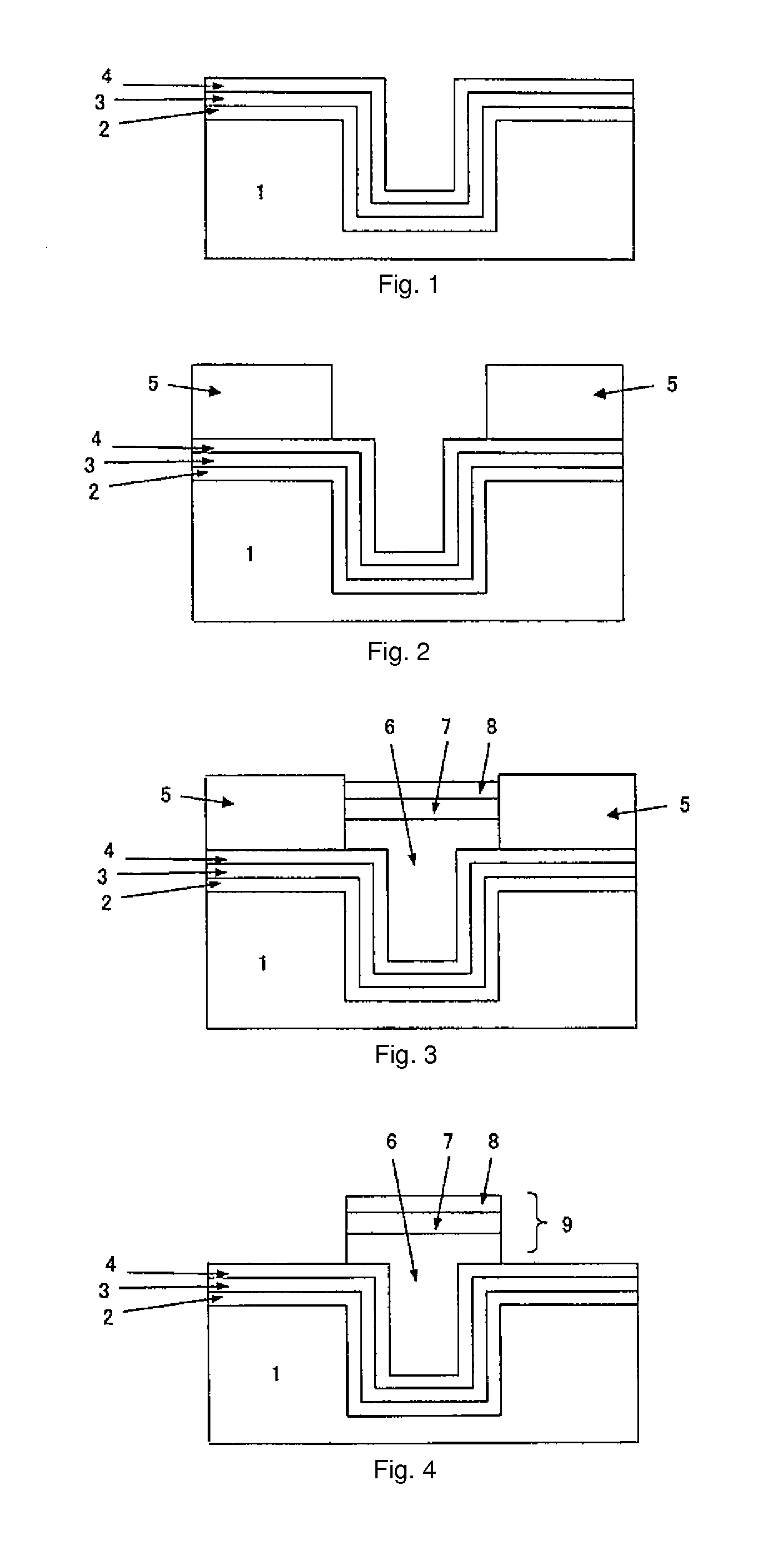
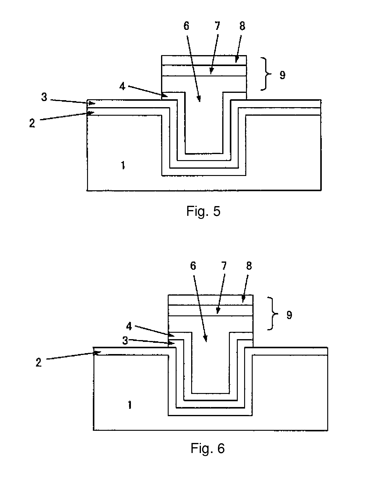
However, since an exposure of copper deteriorates the connection reliability due to causing a surface oxidizing phenomenon, it is the common practice to stack a nickel layer and a solder layer made of an alloy of gold or tin and silver (FIG. 3).
However, in the etching methods as disclosed in Patent Documents 1 to 3, when the copper seed layer formed on the electronic substrate is etched after bump formation, there is a problem of causing a deform of the bump for the reason that a nickel used for the bump formation is etched.
In the existing etching devices, the liquid level of a buffer tank containing a chemical solution is detected and controlled by a sensor and thus generated foam from the etching solution causes the sensor to malfunction.
In addition, the etching solution is circulated using a pump and thus the generated foam causes air entrainment of the pump, leading to a problem in the delivery of the etching solution.
Method used
View moreImage
Smart ImageViewing Examples

Examples
examples
[0075]The invention will hereinafter be described in further detail by Examples and Comparative Examples, which does not limit the present invention. Unless otherwise specifically indicated, % means wt % and “part” or “parts” mean “part or parts by weight”.
Login to View More PUM
| Property | Measurement | Unit |
|---|---|---|
| Selectivity | aaaaa | aaaaa |
Abstract
Object is to provide an etching solution which generates less foam and can etch copper or copper alloy at high selectivity when used in a step of etching copper or copper alloy in an electronic substrate having both of copper or copper alloy and nickel.The etching solution to be used in a step of selectively etching copper or copper alloy in an electronic substrate having both of copper or copper alloy and nickel has, as essential components thereof, (A) a linear alkanolamine, (B) a chelating agent having an acid group in the molecule thereof, and (C) hydrogen peroxide.
Description
BACKGROUND OF THE INVENTION[0001]1. Field of the Invention[0002]The present invention relates to an etching solution for etching copper or copper alloy in an electronic substrate, in particular, an etching solution for selectively etching copper or copper alloy in an electronic substrate having an electrode (bump) made of copper or copper alloy and nickel.[0003]2. Description of the Related Art[0004]In order to improve the performance of electronic devices, their elements have been miniaturized or mounted with high density. However, particularly in semiconductor devices, the miniaturization technology is approaching its limits. Devices with a three-dimensional structure have been put to practical use by using conventional wire bonding, flip chip or bump as a technology of mounting elements with high density. However, there is a demand for further increase in the density. Therefore, TSV technology has been being developed, which is a technology of forming a thin via penetrating throu...
Claims
Login to View More Application Information
Patent Timeline
 IPC IPC(8): C23F1/18
CPCC23F1/18C23F1/34C23F1/44H01L21/32134H01L21/76865H01L21/76898H01L23/481H01L24/03H01L24/05H01L24/11H01L24/13H01L2224/03614H01L2224/03826H01L2224/03912H01L2224/0401H01L2224/05027H01L2224/05166H01L2224/05572H01L2224/05647H01L2224/1146H01L2224/1147H01L2224/13009H01L2224/13083H01L2224/13144H01L2224/13147H01L2224/13155H01L2924/00014H01L2924/12044H01L2924/1461H01L2924/01079H01L2924/00H01L2224/05552
InventorKOJIMA, TSUTOMUKOJI, YUKICHI
OwnerSAMSUNG ELECTRONICS CO LTD