

MEMS device, electronic device, electronic apparatus, and moving object
- Summary
- Abstract
- Description
- Claims
- Application Information
AI Technical Summary
Benefits of technology
Problems solved by technology
Method used
Image

Examples
first embodiment
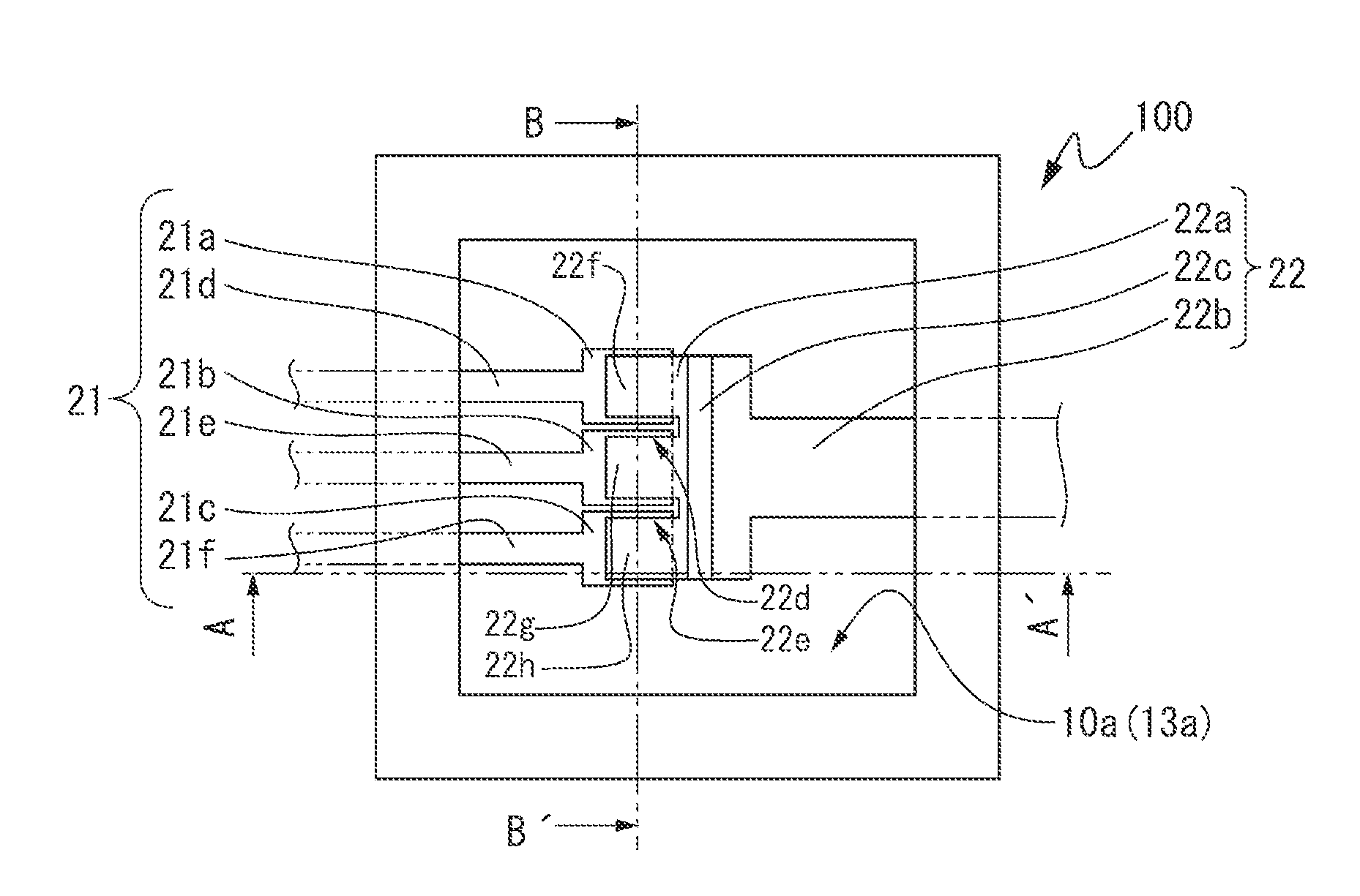
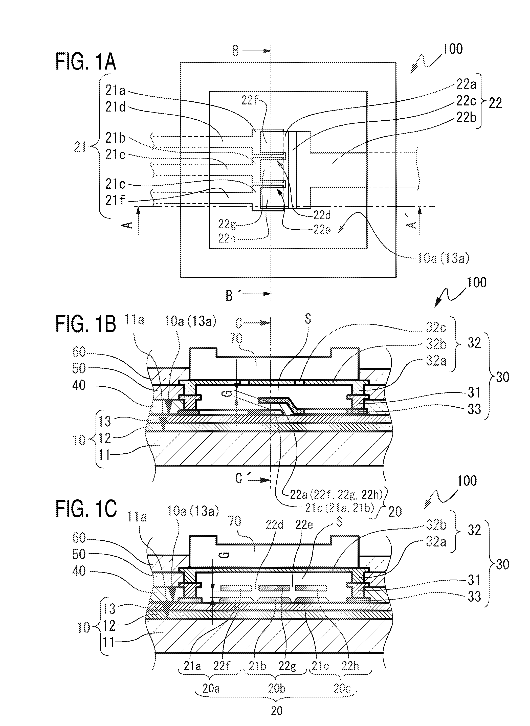
[0041]FIGS. 1A to 1C show a MEMS device according to a first embodiment, in which FIG. 1A is a plan view in a state where a covering layer and a lid, both described later, are removed; FIG. 1B is a cross-sectional view of a portion A-A′ shown in FIG. 1A; and FIG. 1C is a cross-section of a portion B-B′ shown in FIG. 1A, which is also a cross-sectional view of a cross-section of a portion C-C′ in FIG. 1B. As shown in FIGS. 1B and 1C, the MEMS device 100 according to the embodiment includes a substrate 10 composed of a wafer substrate 11, a first oxide film 12 arranged on a principal plane 11a of the wafer substrate 11, and a nitride film 13 arranged on the first oxide film 12. The wafer substrate 11 is a silicon substrate, and the MEMS device 100 is manufactured using a semiconductor manufacturing apparatus and a semiconductor manufacturing method.
[0042]On a principal plane 10a of the substrate 10, that is, on a surface 13a of the nitride film 13, a first conductive layer 21 and a se...
second embodiment
[0066]As an electronic device according to a second embodiment, FIG. 6 shows a form in which the MEMS device 100 according to the first embodiment and a semiconductor device are made into one chip. In an oscillator 1000 as the electronic device shown in FIG. 6, the MEMS device 100 according to the first embodiment and a semiconductor device 200 (hereinafter referred to as IC 200) in which an electronic circuit including an oscillator circuit or a control circuit is configured are integrally arranged.
[0067]Since the MEMS device 100 is a micro device that can be manufactured by a semiconductor manufacturing method using a semiconductor manufacturing apparatus, the IC 200 can be easily formed on the same wafer substrate 11 as that of the MEMS device 100. The IC 200 includes an oscillator circuit that drives the MEMS device 100 and a control circuit that performs driving for frequency fluctuations of the MEMS device 100 or control of output signals to the outside. By forming the IC 200 ...
third embodiment
[0068]As electronic apparatuses according to a third embodiment, a smartphone and a digital still camera including the oscillator 1000 or the gyro sensor 2000 according to the second embodiment will be described.
[0069]FIG. 7 is an external view showing a smartphone 3000. Into the smartphone 3000, the oscillator 1000 (not shown) as a reference clock oscillation source and the gyro sensor 2000 that detects the attitude of the smartphone 3000 are incorporated. By incorporating the gyro sensor 2000, so-called motion sensing is carried out, so that the attitude of the smartphone 3000 can be detected. Detection signals of the gyro sensor 2000 are supplied to, for example, a micro computer chip 3100 (hereinafter referred to as MPU 3100). The MPU 3100 can execute various types of processing according to the motion sensing. In addition, the motion sensing can be utilized by incorporating the gyro sensor 2000 into an electronic apparatus such as a mobile phone, a portable game console, a game...
PUM
 Abstract
Description
Claims
Application Information