Printed circuit board

a printed circuit board and circuit board technology, applied in printed circuit aspects, cross-talk/noise/interference reduction, metallic pattern materials, etc., can solve the problems of emanation of electromagnetic noise, inducing the malfunction of other electronic equipment, and electromagnetic radiation noise generated in these electronic equipments can become not, so as to reduce noise and efficiently return a noise current

Active Publication Date: 2014-09-04
CANON KK
View PDF8 Cites 9 Cited by
  • Summary
  • Abstract
  • Description
  • Claims
  • Application Information

AI Technical Summary

Benefits of technology

[0016]For this reason, an object of the present invention is to provide a printed circuit board which efficiently returns a noise current to a semiconductor device by a capacitor element mounted on the printed circuit board and a planar capacitor formed in the printed circuit board, and can reduce a noise to be emanated.

Problems solved by technology

However, in a high-frequency band, impedance cannot be neglected which originates in parasitic components of the wiring and the planate conductor, and accordingly, potential fluctuations of a power source and a ground are induced by an electric current for supplying an electric charge to the IC / LSI.
The cable connected to this printed circuit board works as an antenna, and results in contributing to emanation of an electromagnetic noise.
On the other hand, the electromagnetic radiation noise generated in these electronic equipments can become not only a cause of inducing a malfunction of a self-circuit, but also a cause of inducing a malfunction of other electronic equipment.
However, in recent years, the semiconductor device such as the IC / LSI progressively tends to use a higher frequency, a conventional configuration is insufficient to reduce the electromagnetic radiation noise originating in the noise current of high frequency generated in the semiconductor device, and has been required to be further improved.
A method of enlarging the second power source conductor plane is considered in order to reduce the noise current which leaks to the first power source conductor plane and efficiently return the noise current to the semiconductor device by the planar capacitor, but there is a limit on the enlargement of the second power source conductor plane because the size of the printed circuit board is restricted.

Method used


Image

  • Printed circuit board
  • Printed circuit board
  • Printed circuit board

Examples


example

Example 1

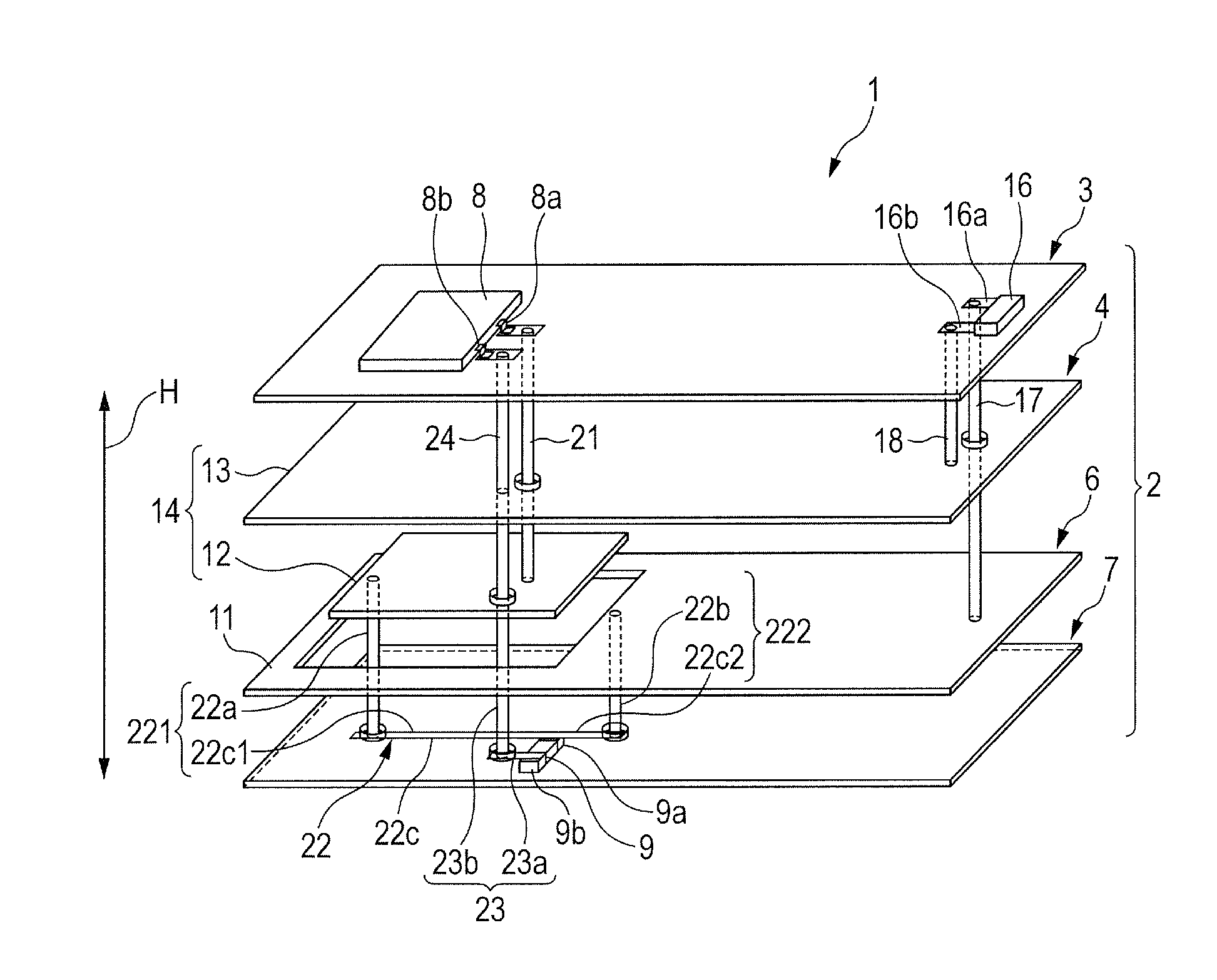
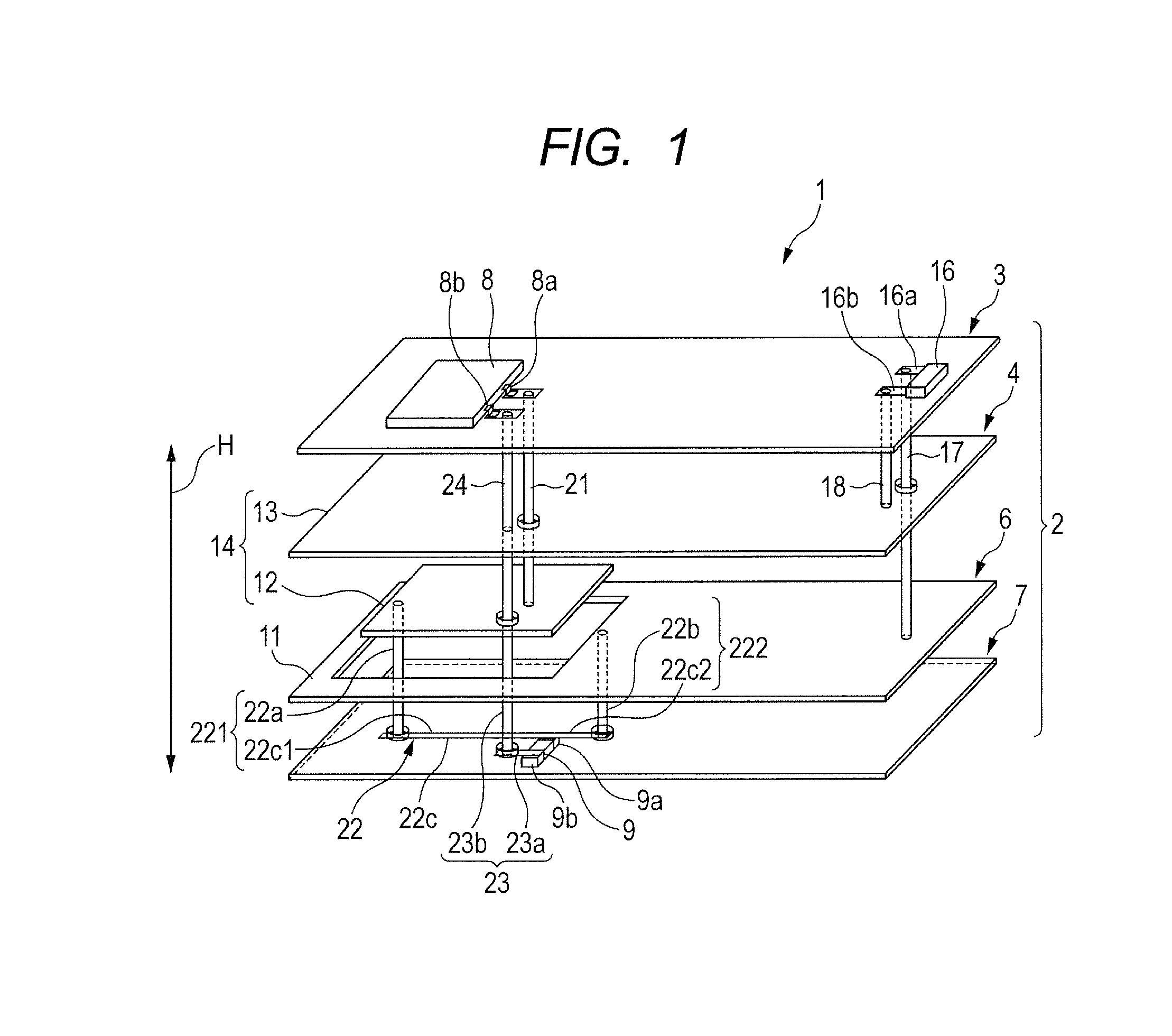
[0076]In order to verify an effect of the above-described embodiment, a simulation was performed by using an electromagnetic field simulator MW-Studio (made by CST AG). FIG. 3A is an exploded perspective view illustrating a printed circuit board according to Embodiment 1 of the present invention, and Embodiment 1 will be described below with reference to FIG. 3A. Incidentally, configurations similar to those in the above-described embodiment are designated by the same reference numerals, and the detailed description will be omitted. The printed circuit board 2A of the printed circuit board 1A which was used for the simulation has a rectangular shape with a short side of 6 cm and a long side of 8 cm.

[0077]The thicknesses of the wiring pattern of the first wiring layer 3, the ground conductor plane 13 of the ground conductor layer 4, the first and second power source conductor planes 11 and 12 of the third wiring layer 6, and the wiring pattern of the fourth wiring layer 7 ar...

example 2

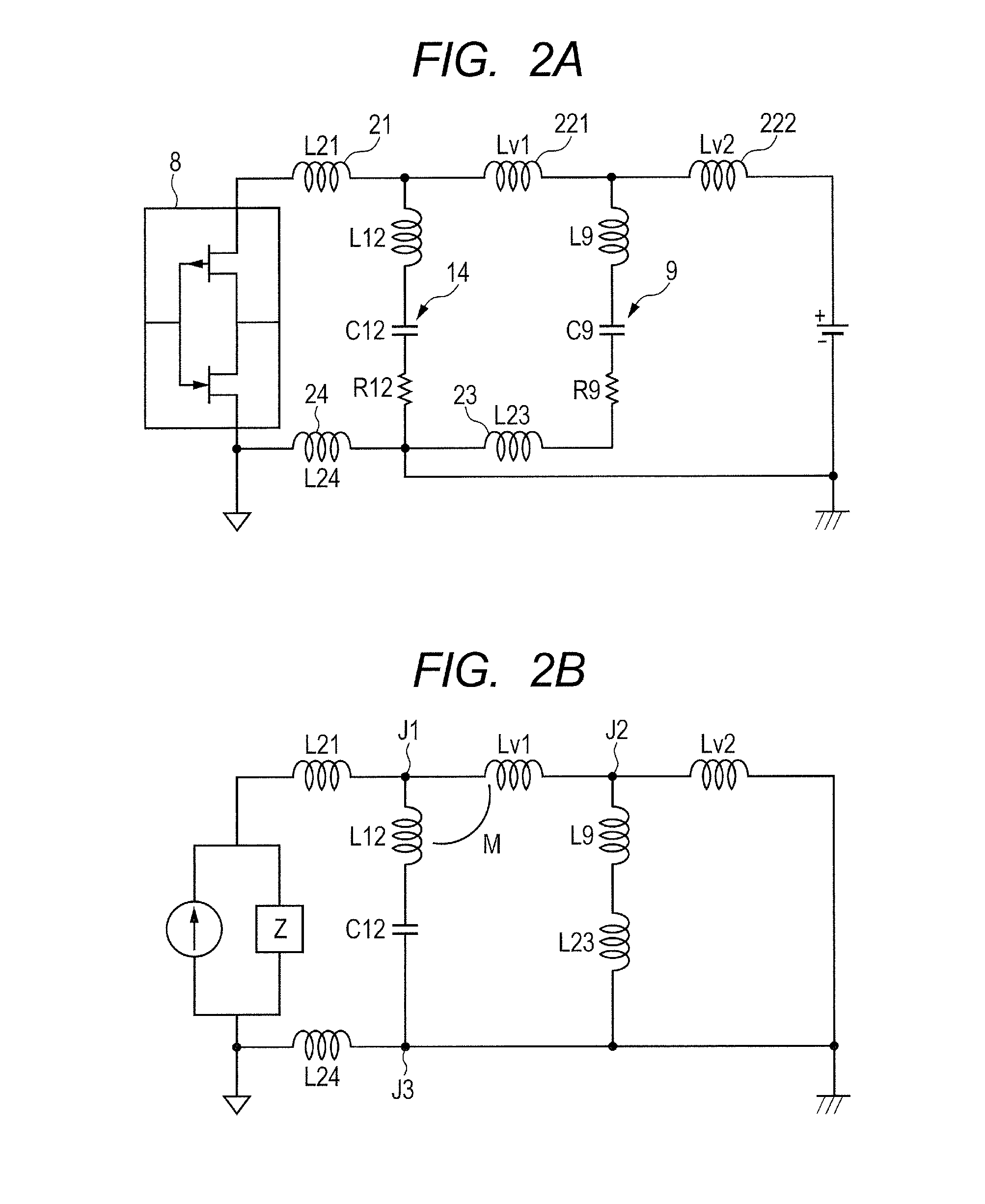
[0083]FIG. 4A is an exploded perspective view illustrating a printed circuit board according to Embodiment 2 of the present invention. Incidentally, configurations similar to those in the above-described embodiment and the above-described embodiments are designated by the same reference numerals, and the detailed description will be omitted. In the above-described Embodiment 1, as illustrated in FIG. 3B, an effect of reducing noise propagation locally decreases with respect to Comparative Example, at 138 MHz and 420 MHz. This cause originates from a parallel resonance of a capacitor element 9 and an inductance of the second connecting conductor 22, and a frequency at which an electric current flowing into the capacitor element 9 increases coincides with the frequency at which the effect of reducing the noise propagation decreases.

[0084]For this reason, in Embodiment 2, the printed circuit board 1B has a resistor element 31 provided therein which is mounted on a fourth wiring layer 7...

example 3

[0087]FIG. 5A and FIG. 5B are cross-sectional views illustrating a printed circuit board according to Embodiment 3 of the present invention. Embodiment 3 will be described with reference to FIG. 5A and FIG. 5B. Incidentally, configurations similar to those in the above-described embodiments are designated by the same reference numerals, and the detailed description will be omitted. As has been described above, in order to directly pass more noise electric current to a planar capacitor 14, it is effective to increase the inductance Lv1 of the connection portion 221 which connects the second power source conductor plane 12 with the capacitor element 9.

[0088]As a method for increasing the inductance Lv1 of the connection portion 221, it is considered to extend a wiring pattern 22c1. However, when the wiring pattern 22c1 faces to the second power source conductor plane 12, a mutual inductance M between the second power source conductor plane 12 and the wiring pattern 22c1 cannot be negl...


PUM


Abstract

A printed circuit board includes a printed circuit board, a semiconductor device mounted on the printed circuit board, a capacitor element mounted on the printed circuit board 2, a ground conductor plane to which a ground terminal of the semiconductor device is connected, and first and second power source conductor planes which are arranged so as not to contact with each other. The second power source conductor plane and the ground conductor plane are arranged so as to oppose to each other to form a planar capacitor. The printed circuit board has a first connecting conductor which connects a power source terminal of the semiconductor device with the second power source conductor plane, and a second connecting conductor which connects the first power source conductor plane with the second power source conductor plane through a first terminal of the capacitor element. Thereby, an electromagnetic radiation noise is reduced.

Description

TECHNICAL FIELD[0001]The present invention relates to a printed circuit board to be used in electronic equipment.BACKGROUND ART[0002]In recent years, a requirement for a digital electronic equipment to have a higher performance is boundless, and a semiconductor integrated circuit (IC / LSI) which is mounted on a printed circuit board and is used as a semiconductor device tends to be more highly integrated and use higher frequency. For this reason, the number of simultaneous switching buffers in the IC / LSI tends to increase, a larger electric current tends to be required, and the switching cycle also tends to become higher frequency. In order to stably operate the IC / LSI mounted on this printed circuit board, a charge supplying function which follows a high-speed operation of the IC / LSI needs to be provided on the printed circuit board. This charge supplying function for the IC / LSI is achieved by a capacitative element connected to the IC / LSI through a wiring or a planate conductor for...

Claims


Application Information

Patent Timeline
Patent Type & Authority Applications(United States)
IPC IPC(8): H01L23/552H01L23/64H01L23/50
CPCH01L23/552H01L23/647H01L23/642H01L23/50H05K1/0225H05K1/0227H05K1/0231H05K1/0234H05K2201/09318H01L2924/0002H01L2924/00
Inventor TAMAKI, HIROTO
Owner CANON KK
Why Eureka
Try Eureka