
Enhanced photoelectron sources using electron bombardment

a photoelectron source and electron beam technology, applied in the field of photoelectron sources, can solve the problems of hampered use of csbr based photoelectron sources for electron beam lithography and related applications, and may be hundreds of monolayers thick csbr films, so as to prolong the lifetime of photocathodes and heightened quantum efficiencies

Active Publication Date: 2014-09-18
THE BOARD OF TRUSTEES OF THE LELAND STANFORD JUNIOR UNIV
View PDF9 Cites 14 Cited by
  • Summary
  • Abstract
  • Description
  • Claims
  • Application Information

AI Technical Summary

Benefits of technology

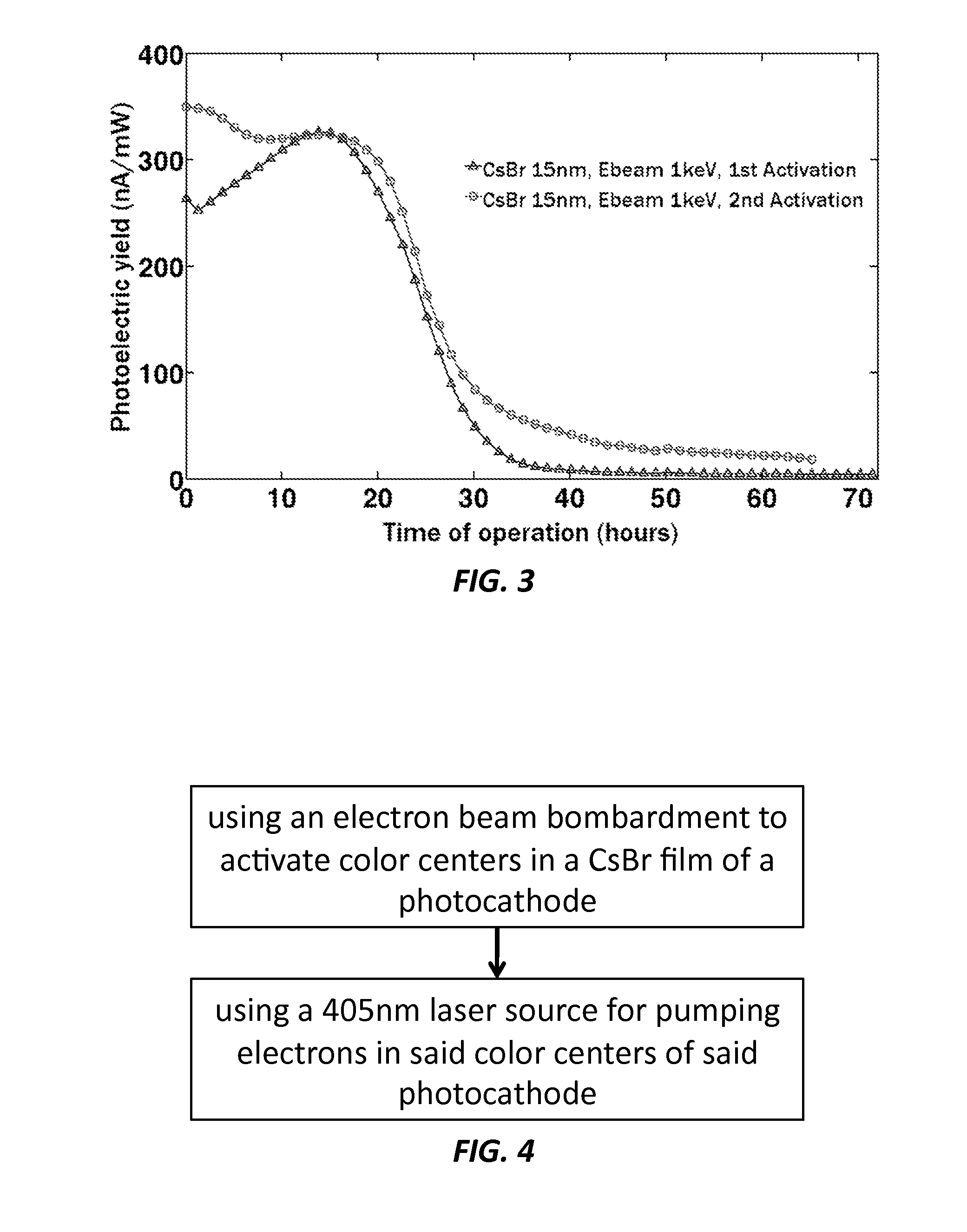
This patent describes a method to achieve better quantum efficiency and longer lifetimes for a photocathode. The method involves using electron beam bombardment to activate color centers in the photocathode and then using a light source to pump these color centers. The light source can be a laser, LED, or incandescent light bulb, with a preferred laser source being a 405 nm laser. The photocathode can be made from a variety of materials and doping methods, with color centers being formed at high energy levels. The method also involves repeated electron beam bombardment to further improve efficiency.

Problems solved by technology

However, only a monolayer of atoms is required to lower the work function of the CsBr / vacuum interface, and the CsBr films may be hundreds of monolayers thick.
The use of CsBr based photoelectron sources for electron beam lithography and related applications has been hampered by the need for bulky and expensive UV lasers to provide the short wavelengths (e.g. 257 nm) necessary to generate sufficiently energetic photons to bring about useful current densities, where “activation” was done by a UV laser having 257 nm wavelength to introduce color center, with energy states inside the band gap.

Method used


Image

  • Enhanced photoelectron sources using electron bombardment
  • Enhanced photoelectron sources using electron bombardment
  • Enhanced photoelectron sources using electron bombardment

Examples


Embodiment Construction

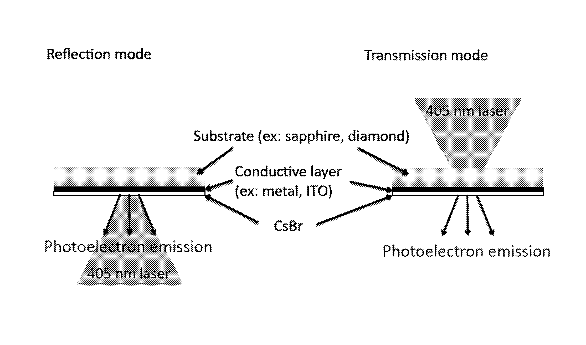
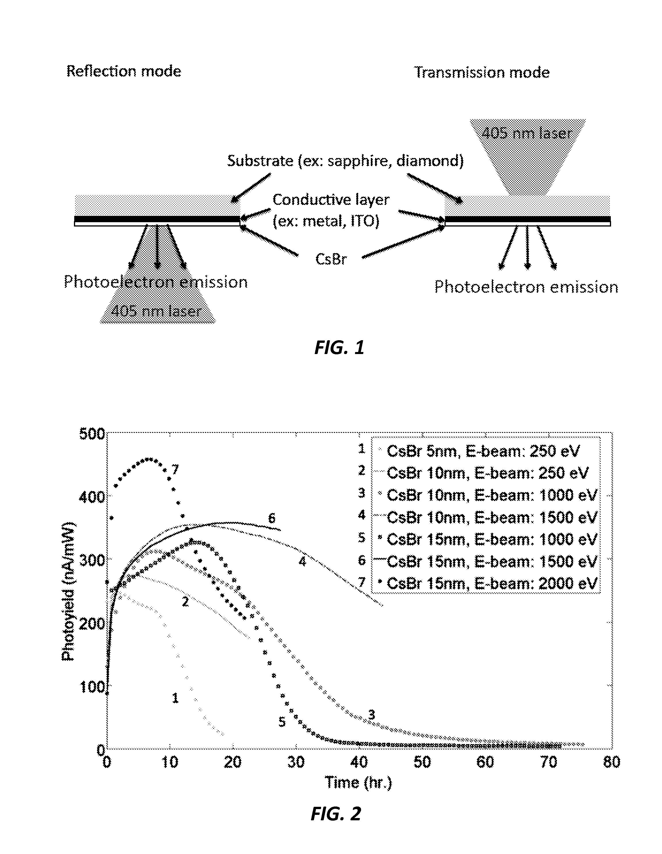
[0018]According to one embodiment, the current invention uses electron beam bombardment to create and activate color centers. Here, the electron beam activated color centers provide more than 10 times higher quantum efficiency than the UV activated color centers with photoelectron emission operated by a 257 nm UV laser. According to one embodiment, the photoelectron emission is operated with a 405 nm laser for pumping electrons, which results in more than a factor of 1000 improvement in quantum efficiency with the electron beam activated color centers than, and with more than a factor of 500 improvement in the photocathode lifetime. In one aspect, the activated color centers can include similar or different color centers, or intra-band states, from UV activated color centers.

[0019]The advantage for this electron beam bombardment activation of color centers for photocathodes is to create paths to use lower photon energy to operate photoelectron emission as an electron beam source. Th...


PUM


Abstract

A method of achieving heightened quantum efficiencies and extended photocathode lifetimes is provided that includes using an electron beam bombardment to activate color centers in a CsBr film of a photocathode, and using a laser source for pumping electrons in the color centers of the photocathode.

Description

CROSS-REFERENCE TO RELATED APPLICATIONS[0001]This application claims priority from U.S. Provisional Patent Application 61 / 790,627 filed Mar. 15, 2013, which is incorporated herein by reference.STATEMENT OF GOVERNMENT SPONSORED SUPPORT[0002]This invention was made with Government support under grant (or contract) no. HSHQDC-12-C-00002 awarded by the Department of Homeland Security. The Government has certain rights in this invention.FIELD OF THE INVENTION[0003]The present invention relates generally to photoelectron sources. More particularly, the invention relates to a method to increase the photoelectron yield of thin film CsBr / metal photocathodes by activation with electron bombardment allowing efficient operation at UV and longer incident light wavelengths.BACKGROUND OF THE INVENTION[0004]Photoelectron emission enhancement mechanisms in metals and semiconductors have been proposed involving the creation of color centers in thin coatings of CsBr films by UV radiation damage. Here,...

Claims


Application Information

Patent Timeline
IPC IPC(8): H01J40/14
CPCH01J40/14H01J40/18
Inventor MALDONADO, JUAN R.CHENG, YAO-TEPIANETTA, PIEROPEASE, R. FABIAN W.HESSELINK, LAMBERTUS
Owner THE BOARD OF TRUSTEES OF THE LELAND STANFORD JUNIOR UNIV
Learn More