Hybrid vertical cavity laser and method of manufacturing the same

a laser and vertical cavity technology, applied in semiconductor lasers, instruments, optical elements, etc., can solve the problem of a somewhat complex manufacturing process for precise alignment between the laser aperture and the optical wave guid

Active Publication Date: 2014-09-18
SAMSUNG ELECTRONICS CO LTD
View PDF0 Cites 5 Cited by
  • Summary
  • Abstract
  • Description
  • Claims
  • Application Information

AI Technical Summary

Benefits of technology

[0010]According to an example embodiment, a hybrid vertical cavity laser includes an optical circuit substrate including a grating having lower refractive index units and a higher refractive index unit alternately arranged in a first direction, the lower refractive index units having a lower refractive index than the higher refractive index unit, and a waveguide guiding light in the first direction, a mesa structure on the optical circuit substrate, the mesa structure including a first-type semiconductor layer, an active layer, a second-type semiconductor layer, and an upper reflective layer sequentially stacked in a second direction perpendicular to the first direction, the first-type semiconductor layer including an exposed portion, a first electrode on the exposed portion of the first-type semiconductor layer, and a second electrode on the upper reflective layer. An overlapped length between the waveguide and a mesa aperture forming an opening through which light produced from the active layer enters the grating is D, a pitch of the grating is p, and 0<D<p.
[0011]The optical circuit substrate may include a first layer, a second layer on the first layer, the second layer including a material having a refractive index higher than that of the first layer and patterned to form the grating and the waveguide, and a dielectric material layer on the second layer, the dielectric material layer including a material having a refractive index lower than that of the second layer.
[0012]The first layer may be formed of silicon oxide, and the second layer may be formed of silicon. The optical circuit substrate may include a silicon on insulator (SOI) substrate, the SOI substrate including a first silicon layer, a silicon oxide layer, and a second silicon layer, the silicon oxide layer may be the first layer, and the second silicon layer may be patterned to form the second layer. The higher refractive index unit may include silicon, and the lower refractive index units may include air.
[0013]A width of lower refractive index units and an interval between neighboring lower refractive index units may be constant. The lower refractive index units may include a first lower refractive index unit and a second lower refractive index unit, the first lower refractive index unit and the second lower refractive index unit having different widths, the first lower refractive index unit and the second lower refractive index unit may be alternately arranged, and the pitch p of the grating is defined as ½ of a pitch between neighboring first lower refractive index units. An interval between neighboring first lower refractive index units and an interval between neighboring second lower refractive index units may be constant. An angle between a side of the mesa structure and the exposed portion of the first-type semiconductor layer may be less than 90°.
[0014]According to example embodiments, a method of manufacturing a hybrid vertical cavity laser includes forming an optical circuit substrate including a grating having a lower refractive index unit and a higher refractive index unit alternately arranged in a first direction, the lower refractive index unit having a lower refractive index than the higher refractive index unit, and a waveguide guiding light in the first direction, forming a laser structure on the optical circuit substrate, the forming a laser structure including stacking a first-type semiconductor layer, an active layer, a second-type semiconductor layer, and an upper reflective layer in order, forming a mesa structure by etching the laser structure in a mesa shape to expose a portion of the first-type semiconductor layer, and forming first and second electrodes on the mesa structure by a single metal deposition process, the first electrode on the exposed portion of the first-type semiconductor and the second electrode on the upper reflective layer.
[0015]The laser structure may be formed by forming a stacked structure on a semiconductor substrate including sequentially stacking the upper reflective layer, the second-type semiconductor layer, the active layer, the first-type semiconductor layer, and a dielectric material layer having a refractive index lower than that of the higher refractive index unit, bonding the stacked structure onto the optical circuit substrate so that the first-type semiconductor layer faces the optical circuit substrate, and removing the semiconductor substrate.

Problems solved by technology

Furthermore, in case that a laser has a mesa structure with a higher aspect ratio, a manufacturing process for precise alignment between the laser aperture and the optical wave guide is somewhat complex.

Method used


Image

  • Hybrid vertical cavity laser and method of manufacturing the same
  • Hybrid vertical cavity laser and method of manufacturing the same
  • Hybrid vertical cavity laser and method of manufacturing the same

Examples


Embodiment Construction

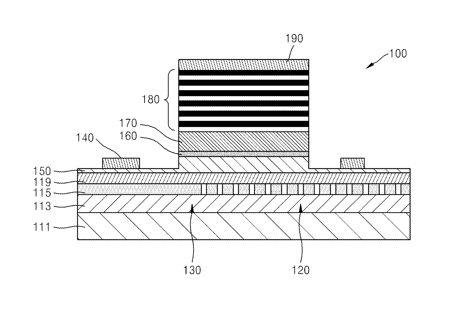
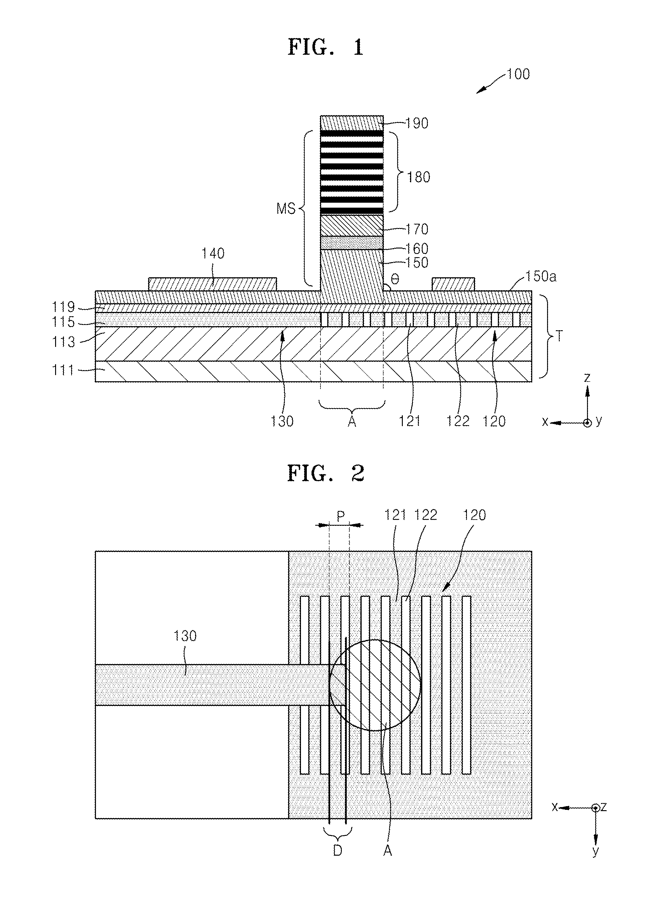
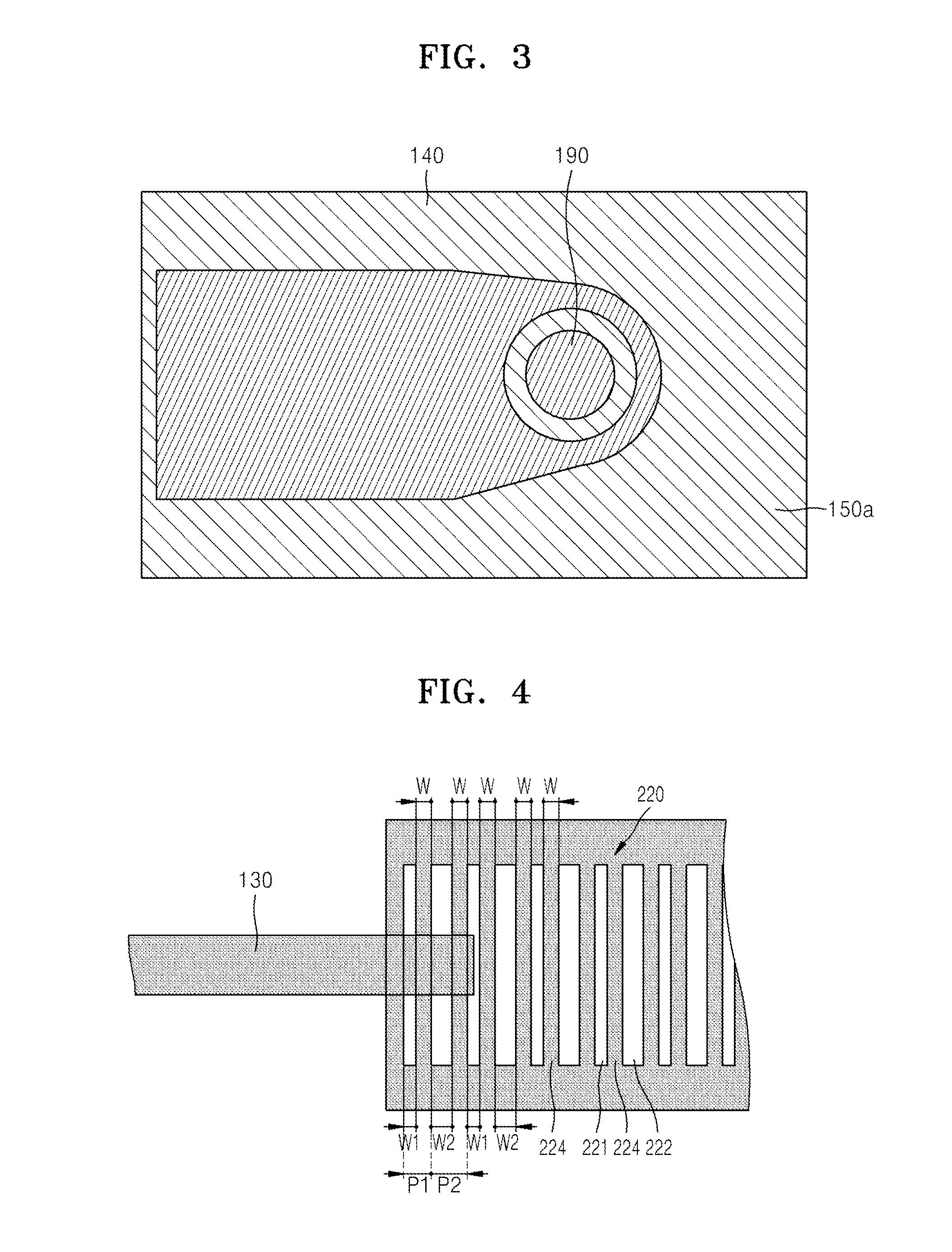
[0030]Example embodiments will be described in detail with reference to the accompanying drawings. In the drawings, like numeral references refer to like components and the dimension of each component may be exaggerated for clarity of description and for convenience.

[0031]It will be understood that, although the terms first, second, third etc. may be used herein to describe various elements, these elements should not be limited by these terms. These terms are used to distinguish one element from another. Thus, a first element discussed below could be termed a second element without departing from the teachings of example embodiments. As used herein, the term “and / or” includes any and all combinations of one or more of the associated listed items.

[0032]The terminology used herein is for the purpose of describing particular example embodiments only and is not intended to be limiting of the present inventive concept. As used herein, the singular forms “a,”“an” and “the” are intended to...


PUM


Abstract

A hybrid vertical cavity laser includes an optical circuit substrate including a grating having refractive index units having a lower refractive index and a higher refractive index with respect to each other that are alternately arranged in a first direction, and a waveguide guiding light in the first direction, a mesa structure on the optical circuit substrate, the mesa structure including a first-type semiconductor layer including an exposed portion, an active layer, a second-type semiconductor layer, and an upper reflective layer sequentially stacked in a second direction perpendicular to the first direction, a first electrode on the exposed portion, and a second electrode on the upper reflective layer. An overlapped length between the waveguide and a mesa aperture forming an opening through which light produced from the active layer enters the grating is D, a pitch of the grating is p, and 0<D<p.

Description

CROSS-REFERENCE TO RELATED APPLICATIONS[0001]This application claims the benefit of Korean Patent Application No. 10-2013-0028820, filed on Mar. 18, 2013, in the Korean Intellectual Property Office, the disclosure of which is incorporated herein in its entirety by reference.BACKGROUND[0002]1. Field[0003]Some example embodiments relate to a hybrid vertical cavity laser and / or a method of manufacturing the same.[0004]2. Description of the Related Art[0005]An optical interconnection technology for data communication by using light has less transmission loss and electromagnetic interference as compared to electrical interconnection. Thus, such an optical interconnection technology is suitable for implementing a system for high-bandwidth, higher speed data communication. Recently, interests in a technology to implement a silicon-based optical integrated circuit have increased.[0006]The silicon-based optical integrated circuit may include several optical devices such as a light source, an...

Claims


Application Information

Patent Timeline
Patent Type & Authority Applications(United States)
IPC IPC(8): H01S5/22H01S5/026
CPCH01S5/026H01S5/22G02B6/12004H01S5/18347H01S5/18361H01S5/11H01S5/183
Inventor KONG, DUANHUAKIM, TAEK
Owner SAMSUNG ELECTRONICS CO LTD
Why Eureka
Try Eureka