Transient electronic devices comprising inorganic or hybrid inorganic and organic substrates and encapsulates

a technology of electronic devices and substrates, applied in the direction of sustainable manufacturing/processing, electric apparatus casings/cabinets/drawers, instruments, etc., can solve problems such as leakage of vapors or fluids, and achieve the effect of effective device fabrication

Active Publication Date: 2014-10-16
THE BOARD OF TRUSTEES OF THE UNIV OF ILLINOIS
View PDF5 Cites 73 Cited by
  • Summary
  • Abstract
  • Description
  • Claims
  • Application Information

AI Technical Summary

Benefits of technology

[0033]In some embodiments, the transient device, or components thereof, are assembled on the substrate via a printing-based or molding-based process, for example, by transfer printing, dry contact transfer printing, solution-based printing, soft lithography printing, replica molding, imprint lithography, etc. In some of these embodiments, therefore, the device, or components thereof, comprise printable semiconductor materials and / or devices. Integration of the device and substrate components via a printing-based technique is beneficial in some embodiments, as it allows for independent processing of semiconductor devices / materials and processing for the substrate. For example, the printing-based assembly approach allows semiconductor devices / materials to be processed via techniques that would not be compatible with some substrates. In some embodiments, for example, the semiconductor devices / materials are first processed via high temperature processing, physical and chemical deposition processing, etching and / or aqueous processing (e.g. developing, etc.), and then subsequently assembled on the substrate via a printing-based technique. An advantage of this approach is that it avoids processing of the semiconductor devices / materials on the substrate in a manner that could negatively impact the chemical and / or physical properties of the substrate, for example, by negatively impacting biocompatibility, toxicity and / or the degradation properties (e.g., degradation rate, etc.) of the transformable substrate. In some embodiments, for example, this approach allows for effective fabrication of the device without exposing the substrate to aqueous processing, for example, processing involving exposure of the transformable substrate to an etchant, a stripper or a developer.

Problems solved by technology

These materials are well known to be good barrier materials for permeation of water vapor in conventional electronics.[4,5,30,31] Previous research[4,31] on encapsulation with PECVD oxide and nitride in organic light-emitting diode (OLED) devices indicates that defects, such as pinholes, are a primary cause of leakage of vapors or fluids.

Method used


Image

  • Transient electronic devices comprising inorganic or hybrid inorganic and organic substrates and encapsulates
  • Transient electronic devices comprising inorganic or hybrid inorganic and organic substrates and encapsulates
  • Transient electronic devices comprising inorganic or hybrid inorganic and organic substrates and encapsulates

Examples


example 1

Inorganic Substrates and Encapsulation Layers for Transient Electronics

Background and Motivation

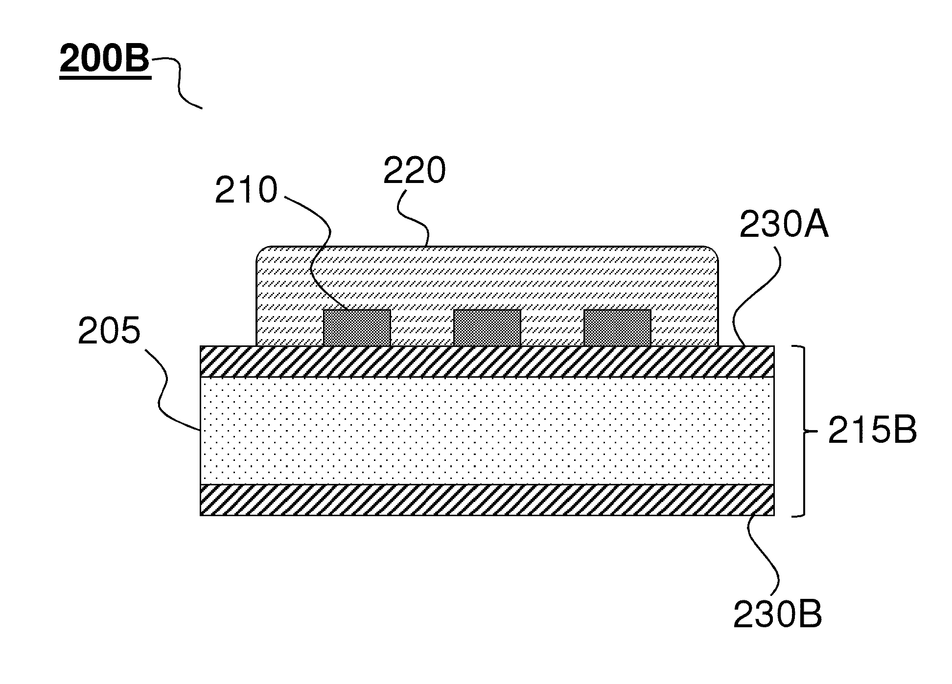
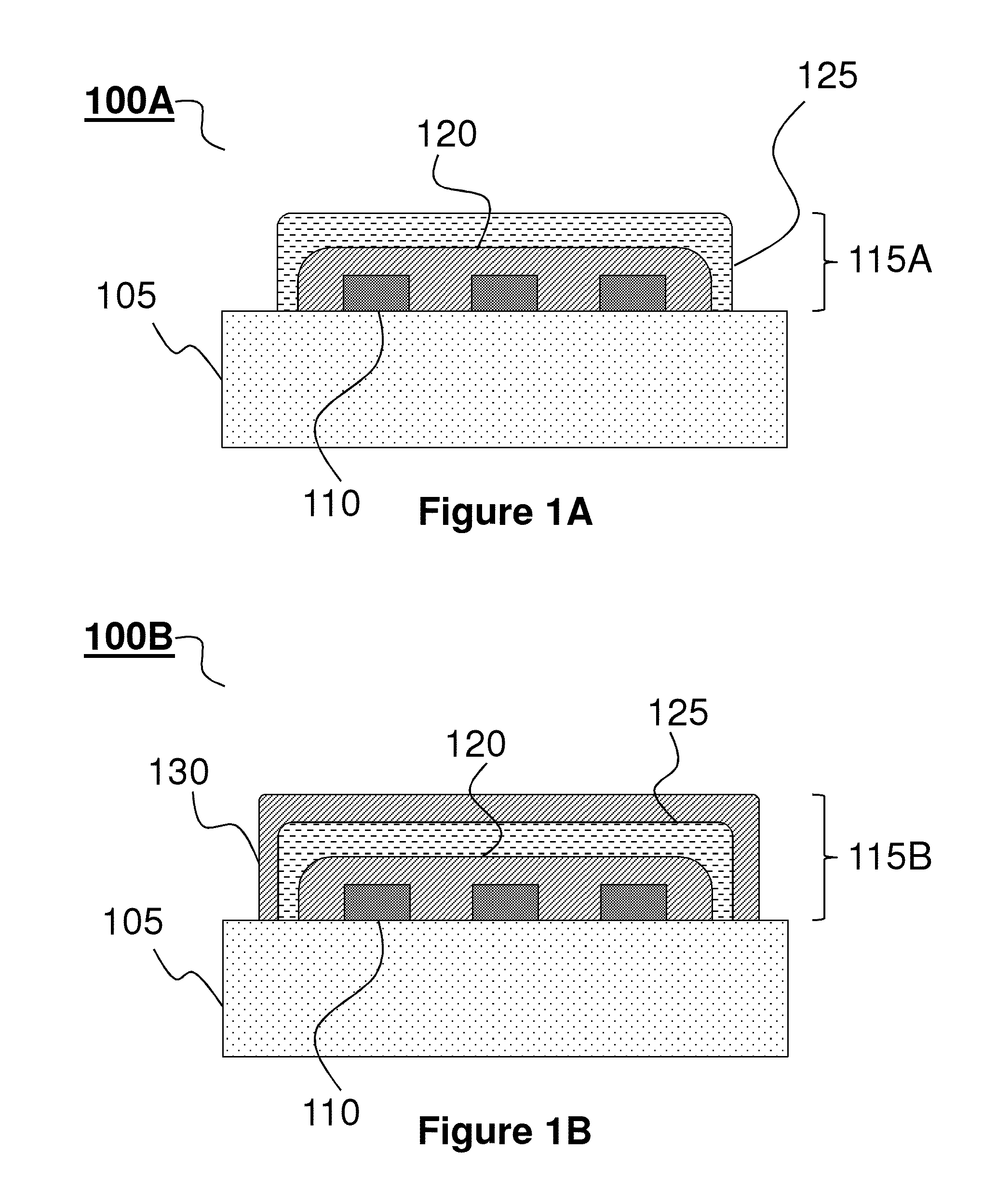
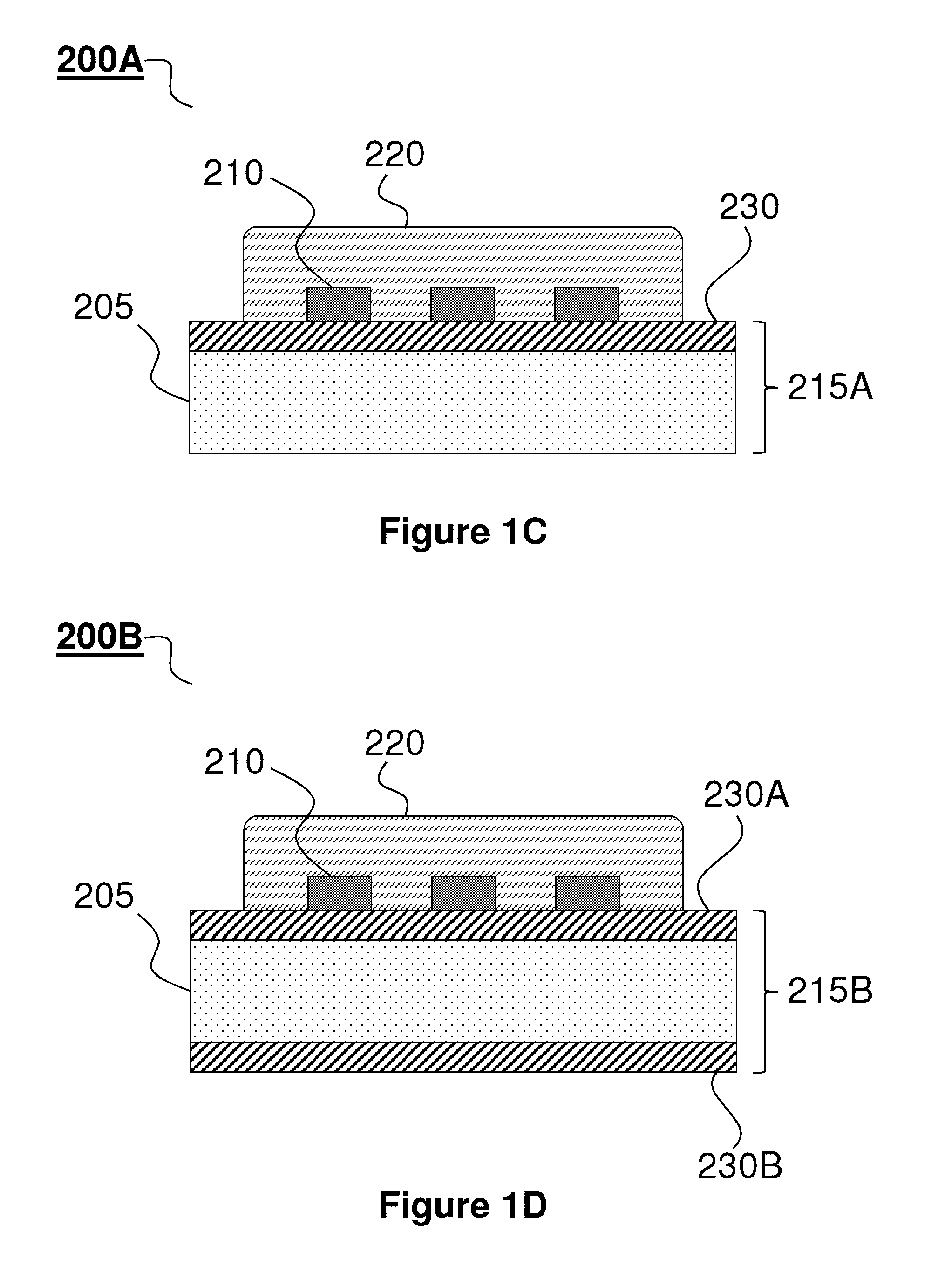
[0134]This example demonstrates a new class silicon-based electronic devices that are physically transient, for example, in the sense that they dissolve or otherwise transform at controlled rates when exposed to water in the environment or the body[1]. In some embodiments, these systems comprise transient materials, such as magnesium for metal electrodes and interconnects, MgO and / or SiO2 for gate and interlayer dielectrics, and single crystal silicon nanomembranes (Si NMs) for semiconductors. In all cases, extensive engineering studies of the key properties, including dissolution mechanisms[2], for each material are important for device engineering. On-going research indicates the ability to enhance / control the dissolution rates of transient components via control over the morphology and chemical compositions of the various functional layers. Additionally, the properties of the aqueous e...

example 2

Inorganic Substrates and Encapsulation Layers for Transient Electronics

[0143]FIG. 6 shows dissolution kinetics of SiO2 in aqueous solution at different pH and temperature (1) SiO2 thermally grown by dry or wet oxidation, (2) SiO2 deposited by plasma enhanced chemical vapor deposition and (3) SiO2 deposited by electron beam evaporation. Calculated (lines) and experimental (symbols) dissolution rates of silicon oxides in buffer solution at different pH (black, pH 7.4; red, pH 8; blue, pH 10; magenta, pH 12) at room (left) and physiological (right, 37° C.) temperature. The thickness was measured by spectroscopic ellipsometry. There was no difference is dissolution rates between thermally grown SiO2 grown by the dry or wet oxidation method.

[0144]FIG. 7A shows measured data (symbols) and numerical fits (lines) for pH-dependent dissolution kinetics of oxides (black, tg-oxide by dry oxidation; red, tg-oxide by wet oxidation; blue, PECVD oxide; magenta, E-beam oxide) at room temperature and...

example 3

Dissolution Behaviors and Applications of Silicon Oxides and Nitrides in Transient Electronics

Background and Motivation

[0168]Silicon oxides and nitrides are key materials for dielectrics and encapsulations in a class of silicon-based high performance electronics that has the ability to completely dissolve in a controlled fashion with programmable rates, when submerged in bio-fluids and / or relevant solutions. This type of technology, referred to as ‘transient electronics’, has potential applications in biomedical implants, environmental sensors and other envisioned areas. The results presented here provide comprehensive studies of transient behaviors of thin films of silicon oxides and nitrides in diverse aqueous solutions at different pH scales and temperatures. The kinetics of hydrolysis of these materials primarily depends on not only pH levels / ion concentrations of solutions and temperatures, but also morphology and chemistry of films determined by the deposition methods and cond...


PUM


Abstract

The invention provides transient devices, including active and passive devices that physically, chemically and/or electrically transform upon application of at least one internal and/or external stimulus. Incorporation of degradable device components, degradable substrates and/or degradable encapsulating materials each having a programmable, controllable and/or selectable degradation rate provides a means of transforming the device. In some embodiments, for example, transient devices of the invention combine degradable high performance single crystalline inorganic materials with selectively removable substrates and/or encapsulants.

Description

CROSS-REFERENCE TO RELATED APPLICATIONS[0001]This application claims the benefit of priority to U.S. Provisional Patent Application No. 61 / 811,603, filed Apr. 12, 2013, U.S. Provisional Patent Application No. 61 / 828,935, filed May 30, 2013, and U.S. Provisional Patent Application No. 61 / 829,028, filed May 30, 2013, each of which is hereby incorporated by reference in its entirety.STATEMENT REGARDING FEDERALLY SPONSORED RESEARCH OR DEVELOPMENT[0002]This invention was made, at least in part, with United States governmental support awarded by the National Science Foundation award no. 1242240 and the Defense Advanced Research Projects Agency award no. W911 NF-11-1-0254. The United States Government has certain rights in this invention.BACKGROUND OF INVENTION[0003]This invention is in the field of transient devices, and relates generally to passive and active devices designed to programmably transform.[0004]Transient devices have potential for a range of important applications. For examp...

Claims


Application Information

Patent Timeline
Patent Type & Authority Applications(United States)
IPC IPC(8): H05K13/00H05K5/06
CPCH05K5/065H05K13/0023A61B5/686H05K1/0286H05K1/0306H05K3/22H05K3/285H05K3/287H05K3/288H05K2201/10151H05K2201/10196H05K2201/10212H05K2203/0271H05K2203/0292H05K2203/0769H05K2203/0776H05K2203/0786H05K2203/175H05K2203/178H01L2924/0002A61B2562/125Y10T428/239Y10T29/49124Y10T137/0318H05K1/0275Y02P70/50H01L2924/00H05K13/00A61M5/44G06K19/0775H05K5/069H01L21/02164H01L21/0217H01L21/02274H01L21/0228H01L21/31111H01L21/31133H01L21/56H01L23/291H01L23/3121H01L23/3192H01L23/49894H01L25/0655H05K1/185H05K2203/17
Inventor ROGERS, JOHN A.KANG, SEUNG-KYUNHWANG, SUKWONCHENG, JIANJUNZHANG, YANFENGYING, HANZE
Owner THE BOARD OF TRUSTEES OF THE UNIV OF ILLINOIS
Why Eureka
Try Eureka