

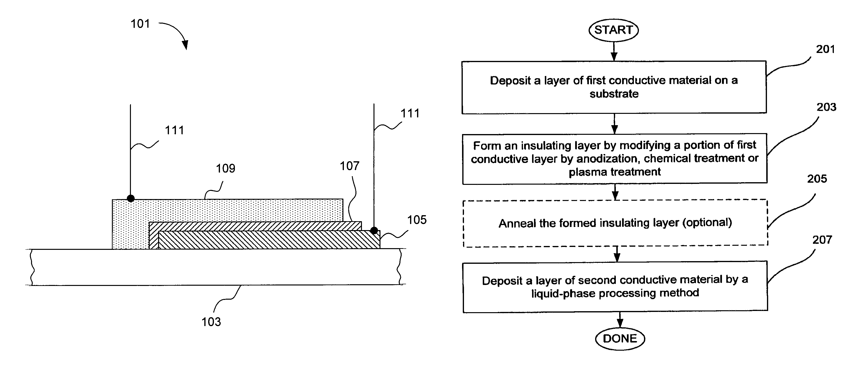
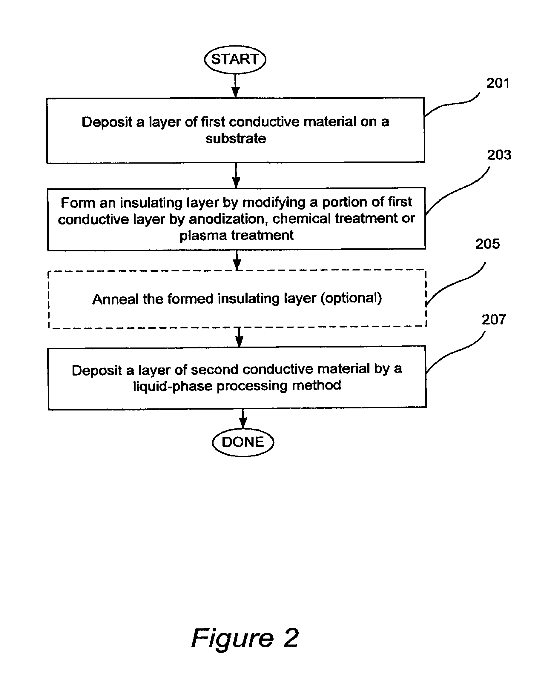
Metal-insulator-metal (MIM) devices and their methods of fabrication
a technology of metal-insulator metal and mim devices, which is applied in the direction of semiconductor devices, hybrid capacitor electrolytes, instruments, etc., can solve the problems of inability to manufacture devices at particular levels of miniaturization, and inability to meet the requirements of the circuit industry, so as to achieve the effect of efficient and inexpensive fabrication methods
- Summary
- Abstract
- Description
- Claims
- Application Information
AI Technical Summary
Benefits of technology
Problems solved by technology
Method used
Image

Examples
example 1
Novel Anodization Process for Forming Ta2O5-δ
[0135]Tantalum film (300 nm thick) was sputtered with a DC sputtering apparatus (Kurt J. Lesker, Model PVD75) on glass substrates. The substrates were not heated. Ta2O5-δ layer was formed by converting the top portion of the tantalum film to Ta2O5-δ by an anodization process which was performed for 60 minutes and was followed by thermal treatment at a temperature of about 300° C. for approximately 20 minutes to form Ta2O5-δ layer having a thickness of about 100 nm. Aluminum metal was then thermally deposited to a thickness of about 150 nm onto the top portion of Ta2O5-δ layer to form MIM diodes with Ta / Ta2O5-δ / Al configuration.
[0136]Traditionally, Ta anodization was carried out with electrolytes containing aqueous acid solution (e.g., citric acid was used). The process of anodization in citric acid was performed as follows: ˜300 nm thick Ta film was dipped into an aqueous solution of citric acid (at approximately 0.01M concentration) and ...
example 2
MIM with Printed Metal Electrodes
[0148]A thin gold (Au) stripe (˜100 nm thick, ˜1 mm wide) was deposited onto a glass substrate. In one example, gold was deposited by electrodeposition. Electrodeposition solution was prepared by dissolving 0.034 g-0.34 g (0.01M-0.1M) of AuCN and 0.0196-0.196 g (0.02-0.2M) of KCN into 15 mL of 0.02-0.2 M KOH aqueous solution. Pulse galvanostatic electrodeposition was carried out using a conventional two-electrode system with Pt wire as a counter electrode. After deposition, the samples were rinsed with DI water and dried by N2 stream.
[0149]In another example, gold electrode was formed by electroless deposition. Electroless plating of Au involved reducing HAuCl4 (0.01M) solution with sodium borohydride (10−3 mol) in the presence of sodium citrate (5×10⁻⁵ M in water) as a capping agent.
[0150]Upon gold deposition, a 100 nm thick Ta film was deposited on top of Au electrode using a DC sputtering PVD apparatus. The Ta layer was converted completely to Ta2...
example 3
MIM Having an Asymmetrical I-V Characteristic with Top PEDOT Electrode
[0155]Ta metal was sputtered using a DC sputtering apparatus either on glass or on plastic substrates to form a 300 nm thick Ta film. Tantalum film was anodized for 30 minutes and was then subjected to thermal treatment at temperature 140° C. for approximately 30 minutes to form 100 nm thick layer of Ta2O5-δ. 3 wt % solution of PEDOT:PSS (H. C. Starck, 4083 or PH500) was drop-cast onto top portion of Ta2O5-δ to form the MIM diodes. Asymmetric I-V characteristic similar to those observed in a PIN silicon diode was obtained. The I-V characteristic of Ta / Ta2O5-δ / PEDOT:PSS is shown in FIG. 6. The rectification ratio (defined as current ratio in both polarities at a given voltage number) at 4V reaches 106. The switch ratio between I(2V) and I(−15V) is 5×10³, which is sufficient to drive a display panel made with a EPD film.
[0156]This experiment was repeated using thermal anneal temperature of between 25° C. and 180° C....
PUM
 Abstract
Description
Claims
Application Information