Attenuation reduction grounding pattern structure for connection pads of flexible circuit board

a flexible circuit board and grounding pattern technology, applied in the direction of printed circuits, printed circuit details, high frequency circuit adaptations, etc., can solve the problems of electromagnetic signal scattering, signal transmission and receipt loss, signal waveform distortion, etc., to reduce the probability of error, reduce reflection loss, excellent effect of impedance match

Active Publication Date: 2014-10-30
ADVANCED FLEXIBLE CIRCUITS
View PDF10 Cites 7 Cited by
  • Summary
  • Abstract
  • Description
  • Claims
  • Application Information

AI Technical Summary

Benefits of technology

[0016]With the technical solution adopted by the present invention, the polarization-direction-varying electrical field induced by the arrangement of the attenuation reduction grounding pattern structure may help reduce reflection loss occurring in the transmission of a high frequency signal, achieve an excellent effect of impedance match, reduce the probability of error in the transmission of a high frequency differential mode signal, and ensure the quality of high frequency signal transmission.
[0017]In an application where a flexible circuit board is combined with a connector, when the differential mode signal lines transmit a high frequency differential mode signal and feed the high frequency differential mode signal to signal connection pins, the grounding pattern structure of the present invention also helps, for the transmission of the high frequency signal by the differential mode signal lines from the extension section to the high frequency connection pads, achieve an effect of impedance matching between the two sections, thereby reducing the probability of error in the transmission of the high frequency differential mode signal and ensuring the quality of high frequency signal transmission.

Problems solved by technology

Although the differential mode signal transmission can greatly improve potential problems that might occur in the transmission of signals, in a practical application, a poor design might result in problems associated with signal reflection, scattering of electromagnetic signals, loss of signal transmission and receipt, and distortion of waveforms of signals.
These problems get severe particularly for flexible circuit boards having reduced substrate thickness.
Factors that cause such problems include: poor matching of characteristic impedance of the differential mode signal lines in extension directions, poor control of excessive stray capacitance effect between high frequency connection pads and a grounding layer, non-matching of characteristic impedance of the differential mode signal lines and the high frequency connection pad.
Further, for example, when a flexible circuit board is plugged into an insertion slot of a female socket connector, the differential mode signal lines and the high frequency connection pads will induce parasitic capacitance and inductance with respect to conductive terminals inside the female socket connector, which cause reflection and loss of the high frequency components of digital signals and thus affect the quality of high speed digital signal transmission.
Further, for example, in an application where a connector is mounted on a flexible circuit board, the differential mode signal lines and the high frequency connection pads will induce parasitic capacitance and inductance with respect to signal connection pins of the connector, which also affect the quality of high frequency signal transmission.
However, for the connection site, as well as neighboring areas, between the differential mode signal lines and the high frequency connection pads provided on a flexible circuit board, due to the line width of the differential mode signal line (the line width being extremely small) and the dimension specifications of the signal connection pins and components of the connector (which are of relatively large sizes as compared to the line width of the signal lines), up to date, there is still no satisfactory solution proposed by the business to ensure the quality of high frequency signal transmission.
Further, in applications where a flexible circuit board is plugged into an insertion slot of a female socket connector and a connector is provided on a flexible circuit board, there is still no satisfactory solution for handling the issues regarding the quality of high frequency signal transmission between the differential mode signal lines and the high frequency connection pads and the conductive terminals of the female socket connector and the signal connection pins of the connector.

Method used


Image

  • Attenuation reduction grounding pattern structure for connection pads of flexible circuit board
  • Attenuation reduction grounding pattern structure for connection pads of flexible circuit board
  • Attenuation reduction grounding pattern structure for connection pads of flexible circuit board

Examples


first embodiment

[0038]Referring to FIG. 7, which is schematic view illustrating an application in which the flexible circuit board 100 according to the present invention is insertable into a female socket connector 7, the female socket connector 7 is provided on a flexible circuit board 71. When the flexible circuit board 100 of the present invention is inserted into an insertion slot 72 of the female socket connector 7, the high frequency connection pads 2a, 2b of the flexible circuit board 100 are positioned to respectively engage conductive terminals 73 mounted in the female socket connector 7.

[0039]Referring to FIGS. 8 and 9, which are respectively an exploded view and a cross-sectional view of a second embodiment of the present invention, the instant embodiment provides a flexible circuit board 200 having a structure that is substantially similar to that of the first embodiment with a difference therebetween residing in that the first end 11 of the component surface 14 of the substrate 1 is pr...

third embodiment

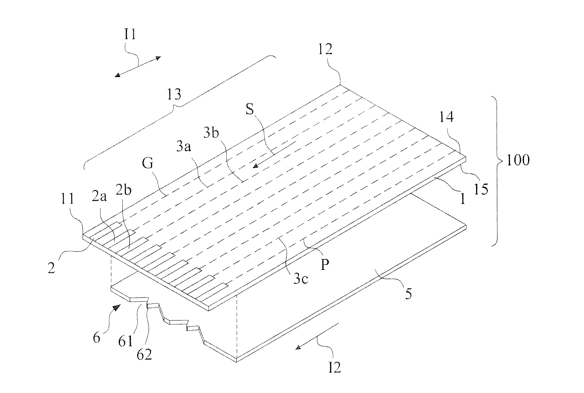
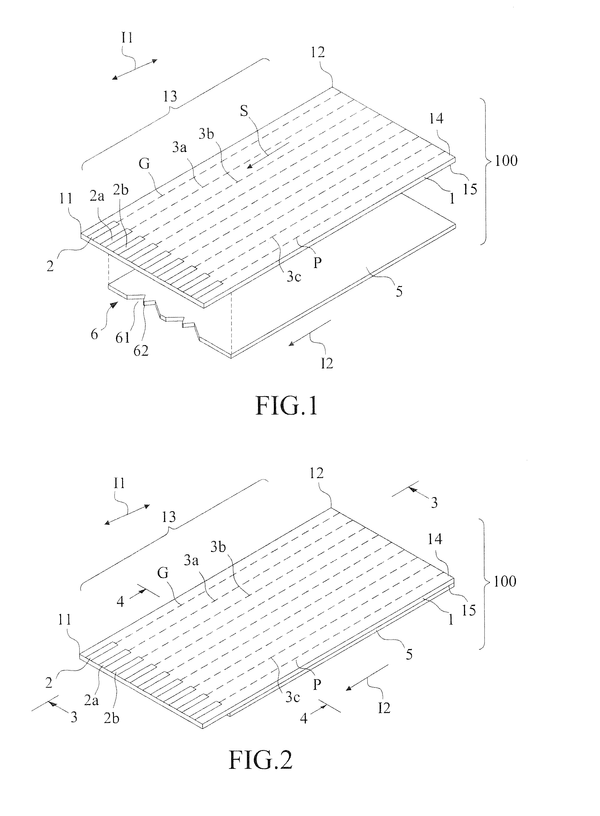
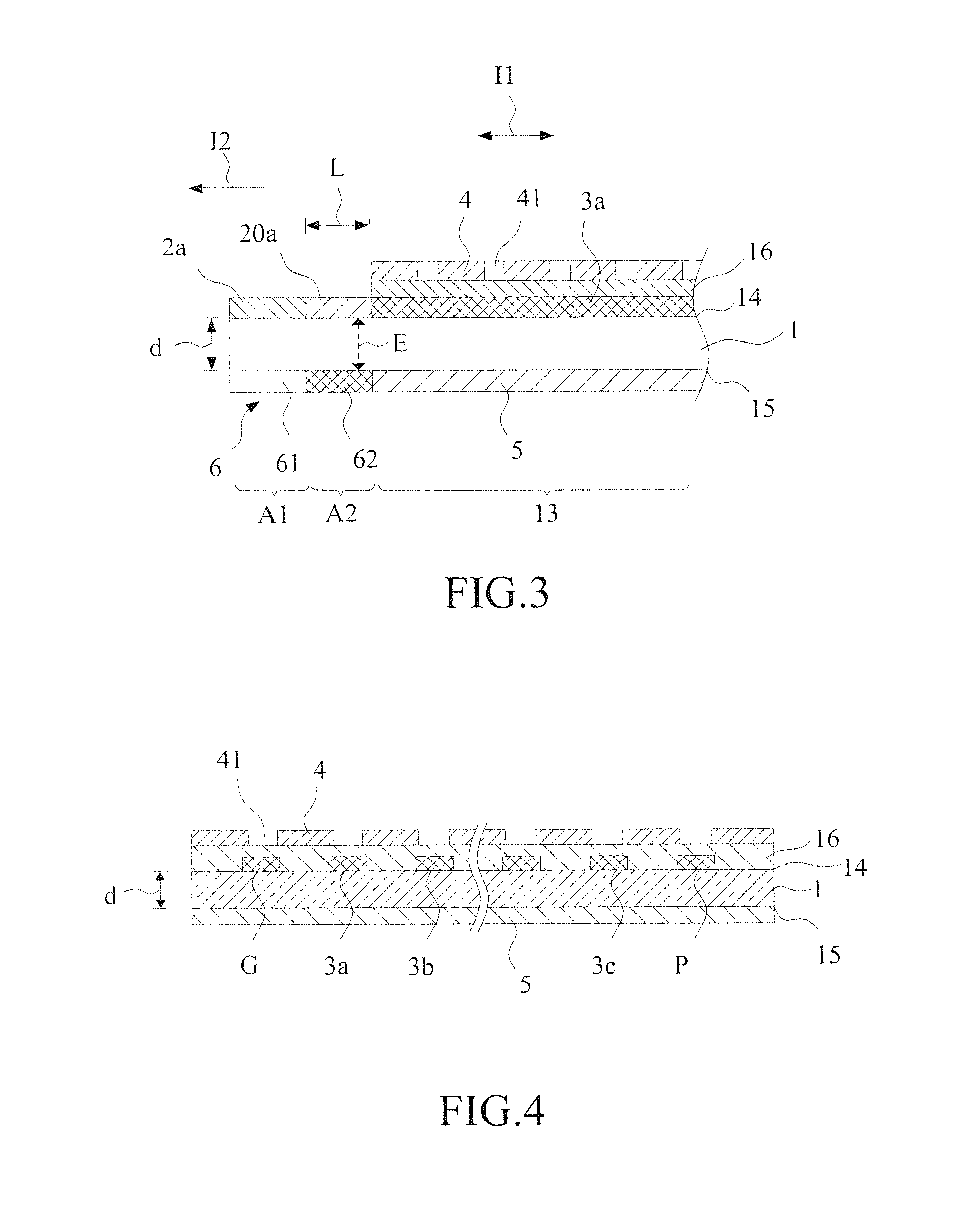
[0044]In the third embodiment, a grounding layer 5 is formed on the grounding surface 15a of the substrate 1. The grounding layer 5 is connected to the grounding line G. Connection of the differential mode signal lines 3a, 3b through the conductive vias 22a, 22b to the high frequency connection pads 2a, 2b is defined as a transition zone A2′.

[0045]The grounding layer 5 comprises a hollowed area 61 and the protruded portion 62 formed in the transition zone A2′ corresponding to the connection pad laying zone A1 and the conductive via arrangement extension sections 21a, 21b to constitute an attenuation reduction grounding pattern structure 6b. The attenuation reduction grounding pattern structure 6b similarly helps the protruded portion 62 and the high frequency connection pads 2a, 2b to form a polarization-direction-varying electrical field in the transition zone A2′ to reduce reflection loss occurring in the transmission of a high frequency signal, achieve an excellent effect of impe...


PUM


Abstract

An attenuation reduction grounding pattern structure for connection pads of a flexible circuit board includes a plurality of high frequency connection pads formed on a component surface of a substrate and a plurality of differential mode signal lines arranged on the substrate and connected to the high frequency connection pads. The substrate has a grounding surface forming a grounding layer. The grounding layer includes an attenuation reduction grounding pattern structure formed at a location corresponding to the transition zone and including a hollowed area and a protruded portion. The protruded portion extends a predetermined length in a direction from the grounding layer toward the high frequency connection pads and along the adjacent high frequency connection pads to reach the transition zone. The protruded portion and the high frequency connection pads form a polarization-direction-varying electric field in the transition zone.

Description

BACKGROUND OF THE INVENTION[0001]1. Field of the Invention[0002]The present invention relates to a structural design for improving the quality of high frequency signal transmission of a circuit board, and in particular to a structure of a flexible circuit board that includes an attenuation reduction grounding pattern structure and the attenuation reduction grounding pattern structure is provided corresponding to connection pads carrying high frequency signals of the flexible circuit board.[0003]2. The Related Arts[0004]Due to the amount of data transmitted through signal lines being increasingly large, electronic devices of the present day requires an increased number of signal transmission lines and also needs the signals to be transmitted in increasingly higher frequencies. Thus, at present, differential mode signal transmission technology has been widely used to reduce electromagnetic interference (EMI). For example, such a technology has been largely used for signals of USB, LVD...

Claims


Application Information

Patent Timeline
Patent Type & Authority Applications(United States)
IPC IPC(8): H05K1/02
CPCH05K1/0253H05K1/0224H05K1/0245H05K1/0227H05K3/3421H05K2201/0949H05K2201/09727H05K2201/10189H05K2201/10689
Inventor TIEN, CHING-CHENGLIN, GWUN-JINCHUO, CHIH-HENGSU, KUO-FU
Owner ADVANCED FLEXIBLE CIRCUITS
Why Eureka
Try Eureka