Semiconductor device

a technology of semiconductor devices and semiconductor chips, applied in semiconductor devices, semiconductor/solid-state device details, electrical devices, etc., can solve the problems of difficulty in establishing insulation between the cooler and the housing, and the general size of the air-cooling cooler, so as to simplify the cooling system, simplify the configuration of the semiconductor device, and enhance the cooling efficiency of the semiconductor chip.

Inactive Publication Date: 2014-10-30
DAIKIN IND LTD
View PDF2 Cites 13 Cited by
  • Summary
  • Abstract
  • Description
  • Claims
  • Application Information

AI Technical Summary

Benefits of technology

[0018]In the first aspect, no electric current flows out of the semiconductor chip (21, 22) through refrigerant. Thus, in a semiconductor device in which a semiconductor chip is cooled by a cooler, an insulating member between the semiconductor chip and the cooler can be omitted, thereby simplifying the configuration of the semiconductor device. This simplified configuration can enhance the cooling efficiency of the semiconductor chip, simplify the cooling system, and reduce an increase in cost of the semiconductor device.
[0019]In the second aspect, the number of wiring members can be reduced. In addition, heat transmitted from the semiconductor chip to peripheral components can be reduced, and the peripheral components can be cooled. Since the semiconductor chip and the peripheral components are cooled by the cooler, the area in cross section of the wiring member can be reduced.
[0020]In the third aspect, the electrode on the semiconductor chip is connected to the cooler, thereby obtaining sufficient cooling when electric current flows in the electrode on the semiconductor chip to generate heat. In particular, since the electrode is configured to have a low electrical resistance, the thermal resistance of the elect

Problems solved by technology

These air-cooling coolers generally tend to be large.
Such a large cooler has difficulty in establishing

Method used


Image

  • Semiconductor device
  • Semiconductor device
  • Semiconductor device

Examples


first embodiment

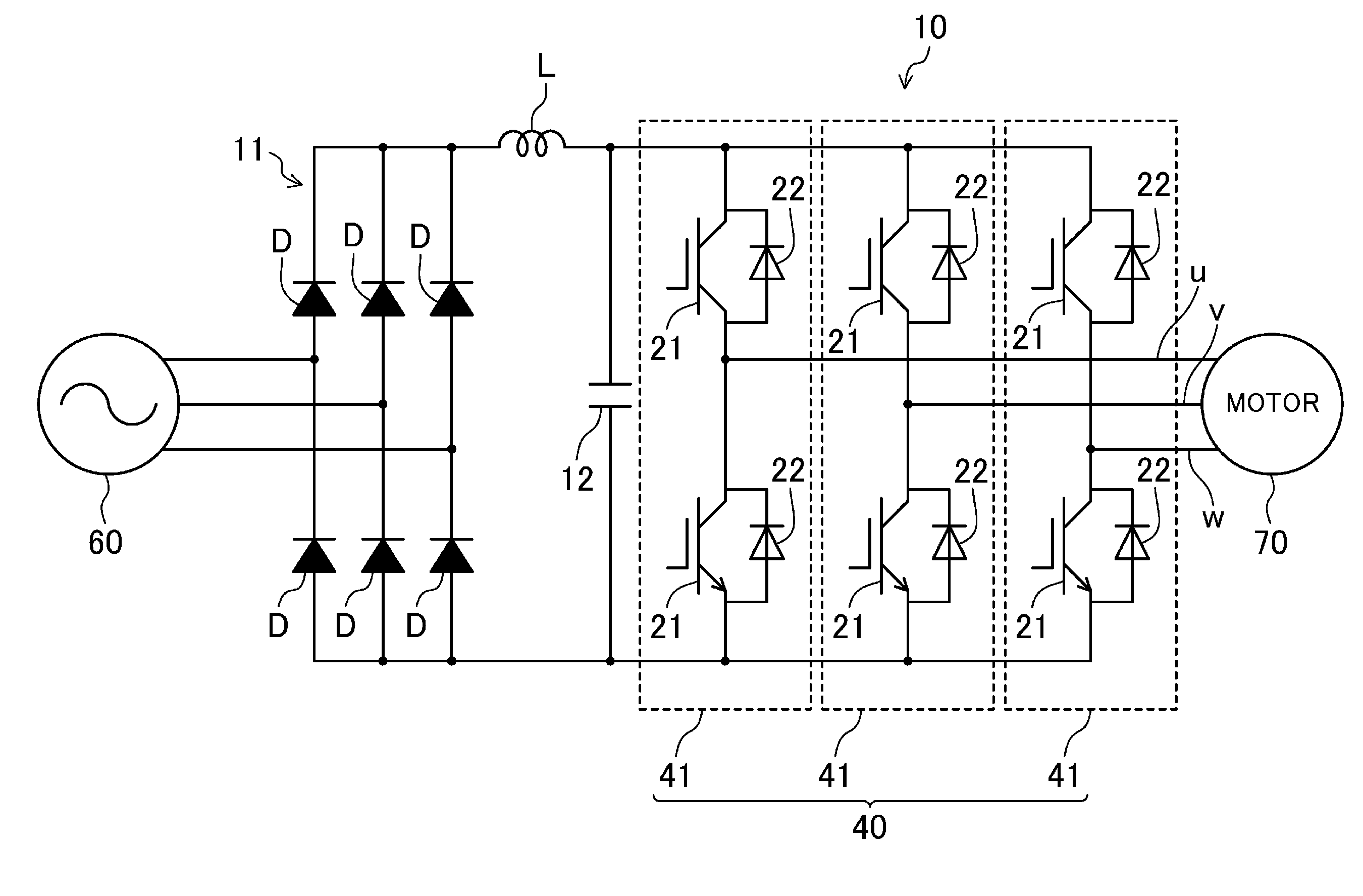
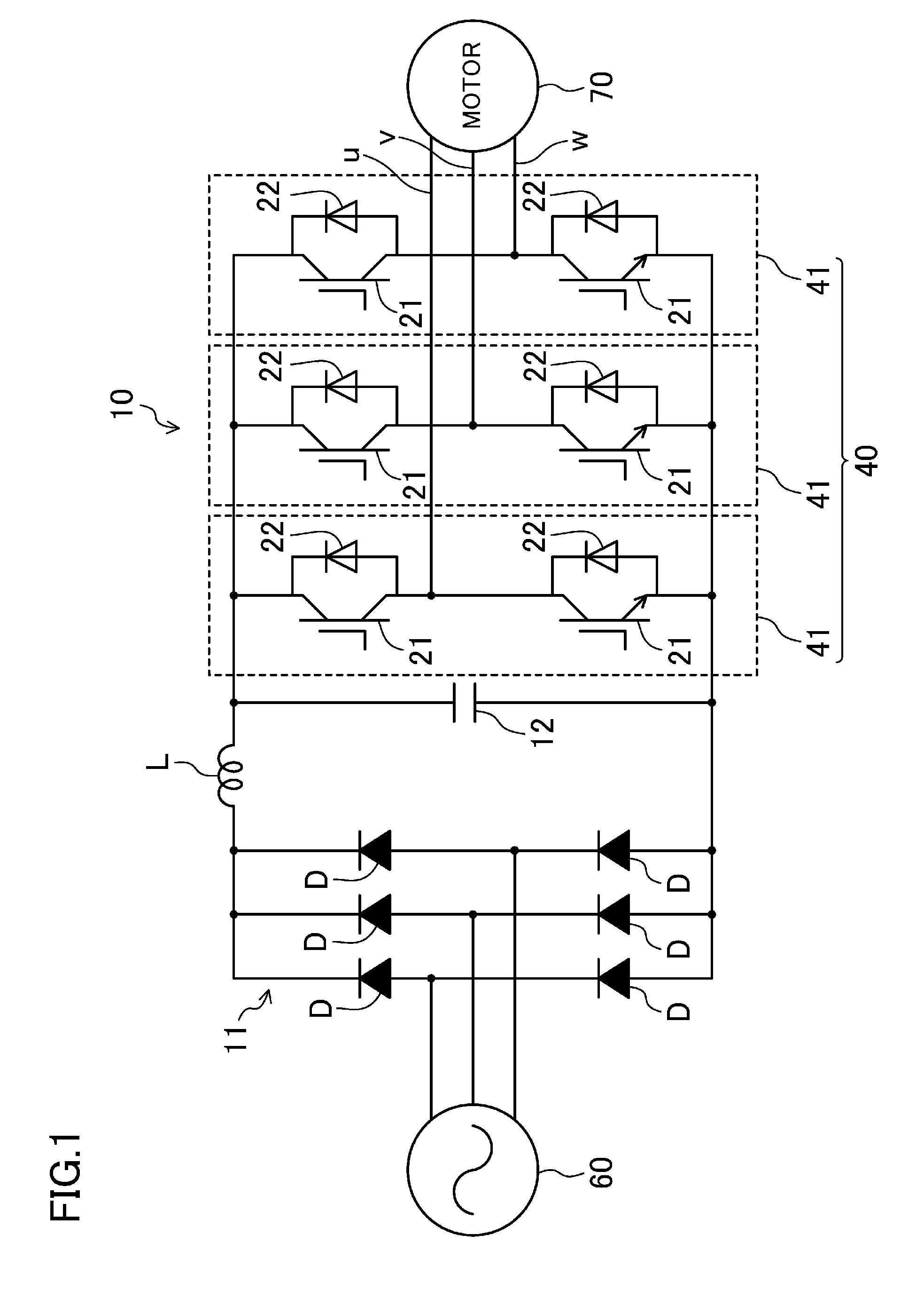
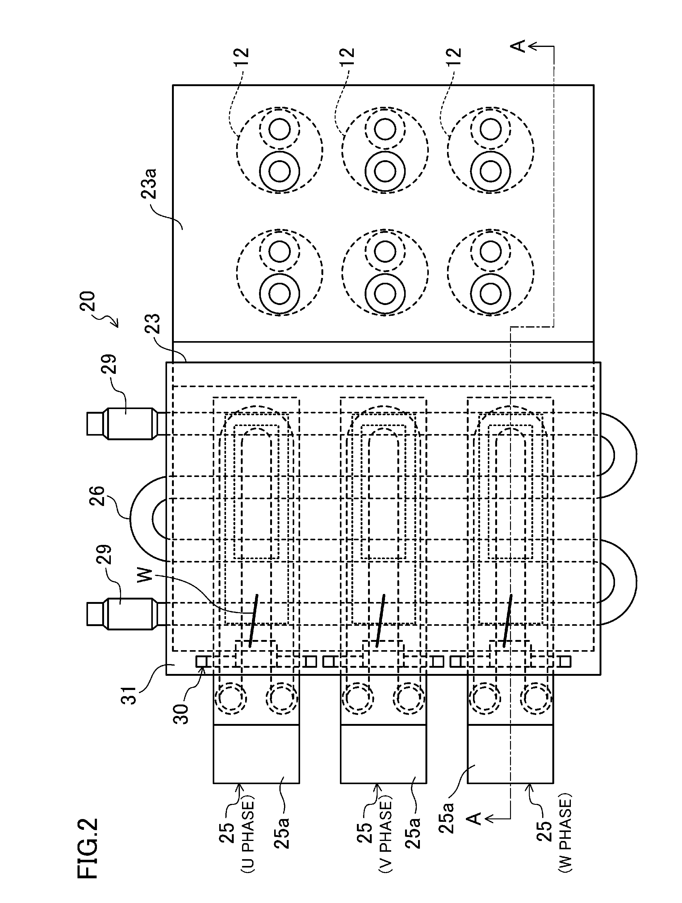
[0032]An example semiconductor device for use in an electric power converter according to an embodiment of the present invention will be described. FIG. 1 is a circuit diagram illustrating an example configuration of an electric power converter (10). FIG. 2 is a top view illustrating a semiconductor device (20) according to a first embodiment. FIG. 3 is a sectional view of the semiconductor device (20) of the first embodiment taken along line A-A in FIG. 2. FIGS. 2 and 3 also illustrate part of components constituting the electric power converter (10) in addition to the semiconductor device (20).

[0033]10)>

[0034]The electric power converter (10) includes a direct-current (DC) power supply (11), a smoothing capacitor (12), and the semiconductor device (20). The DC power supply (11) includes six bridged diodes (D), and performs full-wave rectification on alternating current (AC) input from a three-phase AC power supply (60). The smoothing capacitor (12) is an electrolytic capacitor tha...

second embodiment

[0069]FIG. 6 is a sectional view of a semiconductor device (20) according to a second embodiment. The semiconductor device (20) of the second embodiment is different from that of the first embodiment in the structure of the switching legs (41). In the second embodiment, the vertical direction (e.g., an upper side, a lower side, an upper surface, and a lower surface) of switching devices (21) and other components coincides with the vertical direction in FIG. 6.

[0070]20)>

[0071]FIG. 6 illustrates a W-phase switching leg (41). The other U-phase and V-phase switching legs (41) have similar configurations. In this semiconductor device (20), three output bars (25), one N-phase bar (23), and one P-phase bar (24) are also provided. In the example illustrated in FIG. 6, the switching device (21) located at the left in FIG. 6 is an upper-arm switching device, and the switching device (21) located at the right in FIG. 6 is a lower-arm switching device. Connection of each of the bus bars (23, 24...

embodiment

Advantages of Embodiment

[0077]In the second embodiment, each of the terminals of the switching devices (21) and the freewheeling diodes (22) is also electrically connected to any one of the bus bars (23, 24, 25) with the solder (28), electric current flows in the bus bars (23, 24, 25) depending on switching of the switching devices (21).

[0078]In addition, each of the switching devices (21) and the freewheeling diodes (22) is thermally connected to any one of the bus bars (23, 24, 25) with the solder (28). Thus, the switching devices (21) and the freewheeling diodes (22) dissipate heat to the refrigerant and are cooled in the bus bars (23, 24, 25) connected to the switching devices (21) and the freewheeling diodes (22).

[0079]Thus, in the second embodiment, advantages similar to those of the first embodiment can be obtained.

Other Embodiments

[0080]Refrigerant does not need to flow in all the bus bars (23, 24, 25). Selection of one of the bus bars (23, 24, 25) in which refrigerant is to...


PUM


Abstract

In a semiconductor device in which a semiconductor chip is cooled by a cooler, an insulating member between a semiconductor chip and a cooler is omitted in order to simplify the configuration. A cooler (23, 24, 25) for performing heat exchange between a semiconductor chip (21, 22) and a refrigerant is provided. The refrigerant is non-conductive. The semiconductor chip (21, 22) and the cooler (23, 24, 25) are connected to each other through a conductive connection component (28) or are directly connected to each other.

Description

TECHNICAL FIELD[0001]The present invention relates to semiconductor devices in which semiconductor chips are cooled by coolers.BACKGROUND ART[0002]Some insulated gate bipolar transistors (IGBTs) used in, for example, inverter circuits are cooled in air-cooling or water-cooling coolers (see, for example, Patent Document 1).[0003]These air-cooling coolers generally tend to be large. Such a large cooler has difficulty in establishing insulation between the cooler and a housing accommodating, for example, an IGBT and an inverter circuit. In a water-cooling cooler, since water has conductivity, an IGBT for use in so-called high-power applications needs electrical insulation between a semiconductor chip constituting the IGBT and a cooler. Thus, in each of the cases of employing an air-cooling cooler and of employing a water-cooling cooler, an insulating member is typically provided between a semiconductor chip and a cooler (see, for example, Patent Document 1).CITATION LISTPatent Document...

Claims


Application Information

Patent Timeline
IPC IPC(8): H01L23/46
CPCH01L23/46H01L23/473H01L23/4334H01L23/49562H01L23/49575H01L2224/48091H01L2924/3011H01L2924/30107H01L23/492H01L2924/13055H01L2924/1305H02M7/003H01L2924/00014H01L2924/00
Inventor ZHOU, YUEQIANGMAEDA, TOSHIYUKI
Owner DAIKIN IND LTD
Why Eureka
Try Eureka