
Method for Patterned Doping of a Semiconductor

Active Publication Date: 2014-10-30
NATCORE TECH
View PDF1 Cites 5 Cited by
  • Summary
  • Abstract
  • Description
  • Claims
  • Application Information

AI Technical Summary

Benefits of technology

The patent describes a method for creating patterned doping on a semiconductor substrate. The method involves printing a polymeric material on the substrate to prevent the deposition of a liquid phase deposition material, and then depositing the liquid phase deposition material on the substrate. The polymeric material is then removed, and a dopant is diffused into the substrate. The deposition of the dopant is impeded by the liquid phase deposition material, leaving behind patterned doping regions where the liquid phase deposition material was not present. The method may be repeated to create further doping regions. This approach allows for precise patterning of doping on semiconductors, which can be useful in various applications.

Problems solved by technology

Screen printing and firing technology imposes limitations on solar cell efficiency improvements due to a restriction on emitter thickness.
When the emitter thickness is not sufficient, diffusion of the contact metal during firing may exceed the emitter depth leading to electrical shunting through the pn junction.
Furthermore, a thin emitter usually implies a lower level of doping which can lead to poor electrical contact between the emitter and the metal contact.
Although the use of a selective emitter has proved to be effective in improving PV cell efficiency, implementation of a selective emitter in practice, is quite complicated.
However, this process requires that the substrate be subjected to an expensive high temperature oxidation.
This additional high temperature heating may cause defects that may be detrimental to charge carrier lifetime and cell performance.
However, this process requires a vacuum plasma treatment of the substrate.
However, electrochemical treatments involve a high degree of equipment complexity to permit electrical contact to substrates.

Method used


Image

  • Method for Patterned Doping of a Semiconductor
  • Method for Patterned Doping of a Semiconductor
  • Method for Patterned Doping of a Semiconductor

Examples


experimental example

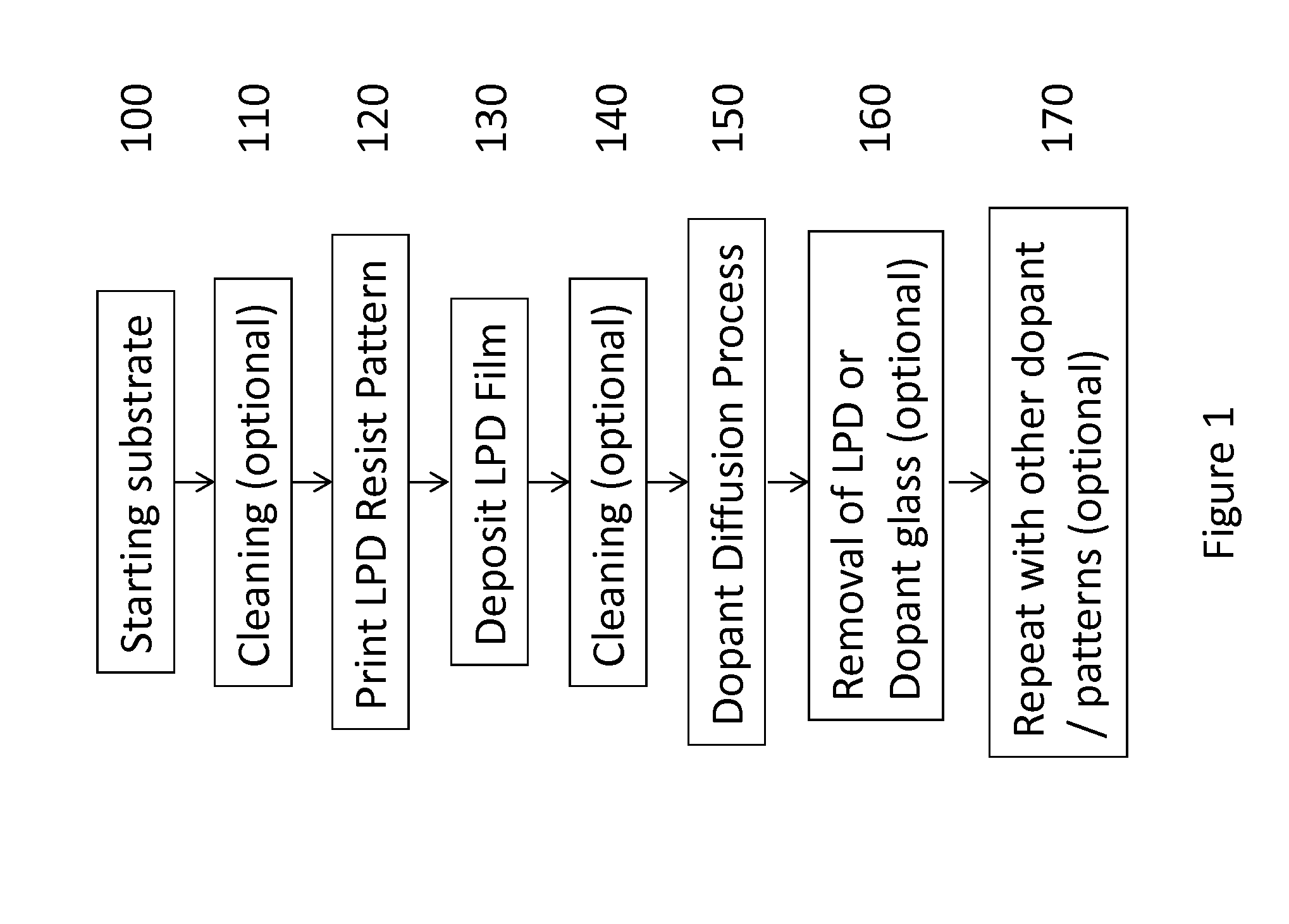
[0043]The following examples are included to demonstrate particular aspects of the present disclosure. It should be appreciated by those of ordinary skill in the art that the methods described in the examples that follow merely represent illustrative embodiments of the disclosure. Those of ordinary skill in the art should, in light of the present disclosure, appreciate that many changes can be made in the specific embodiments described and still obtain a like or similar result without departing from the spirit and scope of the present disclosure.

example 1

[0044]This example demonstrates the capability of a patterned film of LPD silicon dioxide to act as a diffusion barrier for a POCl3 dopant diffusion.

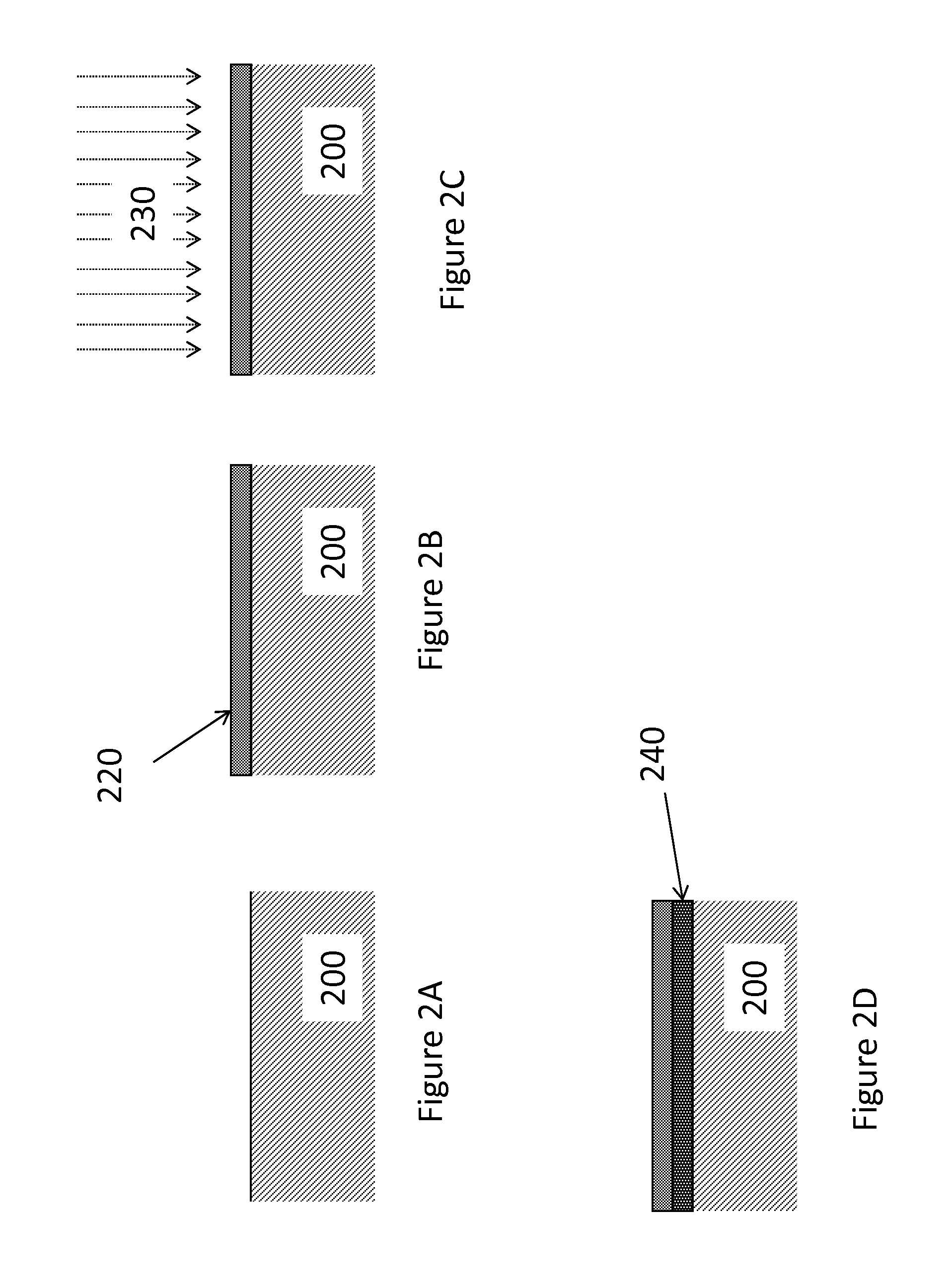
[0045]125 mm×125 mm p-type silicon wafers with pyramidal surface texture were cleaned by dipping in 1:10 HF:Water for 10 minutes followed by extensive rinsing in deionized water.

[0046]A polymer resist ink is formulated by dissolving a polymer composed of approximately 88% vinylbutyral, 11% vinylalcohol, and 1% vinylacetate monomer units in butoxyethanol at 17 weight% polymer. A test pattern of polymer resist ink is screen printed on the wafers followed by baking at 70° C., producing areas on the wafers with and without coverage of the polymer.

[0047]An LPD stock solution is created by adding 70 g of high purity fumed silica per 1 liter of 35 wt % H2SiF6 aqueous solution. The mixture is stirred for 12 hours at room temperature, at which point excess silica is filtered out, yielding a saturated solution. For a given deposition, 1100 g of t...

example 2

[0052]This example demonstrates the capability of a patterned film of LPD silicon dioxide to act as a diffusion barrier for a spin on dopant diffusion.

[0053]Silicon wafers are processed as in example 1 to yield patterned LPD silicon dioxide films. Instead of a POCl3 based dopant diffusion, the wafers are spin coated with Honeywell P-8545 spin-on phosphorous dopant. After a 250° C. bake for 15 minutes to ensure a dry coating, the coatings are annealed at 950° C. for 16 minutes in air in a rapid thermal processor.

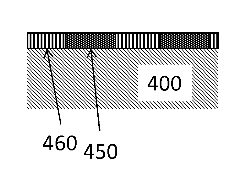
[0054]Resistivity of the wafers was measured using a four point probe test. The resistivity on areas where the LPD was absent is labeled Rc, and the resistivity in areas where LPD is present is labeled Re. Table 2A shows the results of these measurements for three samples that had received different LPD treatments.

TABLE 2AApprox SiO2thicknessSampleLPD Treatment(nm)Rc (ohm / sq)Re (ohm / sq)E2-145° C. / 8 minutes1027.1 (n-type) 48.7 (n-type)E2-245° C. / 15 minutes1837.1 (n-type)150.2 ...


PUM


Abstract

A method for an improved doping process allows for improved control of doping concentrations on a substrate. The method may comprise printing a polymeric material on a substrate in a desired pattern; and depositing a barrier layer on the substrate with a liquid phase deposition process, wherein a pattern of the barrier layer is defined by the polymeric material. The method further comprises removing the polymeric material, and doping the substrate. The barrier layer substantially prevents or reduces doping of the substrate to allow patterned doping regions to be formed on the substrate. The method can be repeated to allow additional doping regions to be formed on the substrate.

Description

RELATED APPLICATIONS[0001]This application claims the benefit of U.S. Provisional Patent Application No. 61 / 815,524, filed on Apr. 24, 2013, which is incorporated herein by reference.FIELD OF THE INVENTION[0002]This invention relates to methods and systems for patterned doping of a substrate. More particularly, to pattern doping of a substrate for solar cells.BACKGROUND OF INVENTION[0003]A crystalline silicon photovoltaic (PV) cell typically has a first surface operable to receive light and a second surface opposite the first surface. The first surface is doped to form the emitter of the PV cell and has a plurality of electrical contacts formed therein. The second surface has at least one electrical contact.[0004]The first contacts are typically formed as a plurality of parallel spaced apart “fingers” that extend across the entire first surface. The fingers are formed by screen printing a metallic paste onto the first surface in a desired pattern. The metallic paste is fired by high...

Claims


Application Information

Patent Timeline
IPC IPC(8): H01L21/223H01L31/18
CPCH01L31/18H01L21/223H01L31/068H01L31/1804Y02E10/547Y02P70/50
Inventor LEVY, DAVID H.MARGADONNA, DANIELEFLOOD, DENNISAHEARN, WENDY G.TOPEL, JR., RICHARD W.ZUBIL, THEODORE
Owner NATCORE TECH
Learn More