Method for Forming Metal Silicide Layers

a metal silicide and layer technology, applied in the field of metal silicide layer formation, can solve the problem of increasing the risk of emitter shunting

Active Publication Date: 2014-11-13
INTERUNIVERSITAIR MICRO ELECTRONICS CENT (IMEC VZW) +2
View PDF7 Cites 4 Cited by
  • Summary
  • Abstract
  • Description
  • Claims
  • Application Information

AI Technical Summary

Benefits of technology

[0007]Certain inventive aspects relate to a method for forming a patterned metal silicide layer, e.g. nickel silicide layer, on a surface of a silicon substrate, wherein the risk of metal, e.g. nickel, spiking is avoided or substantially reduced as compared to prior art methods. A method according to one inventive aspect can be applied on a textured silicon surface, such as a textured surface of a photovoltaic cell, without substantially damaging the surface texture. In one aspect, a method can advantageously be used for selectively forming electrical contacts at the front side of a photovoltaic cell, e.g. in openings created in a dielectric layer, e.g. an antireflection coating, even when such openings are created by means of laser ablation, and without deteriorating the surface passivation quality of the dielectric layer.

Problems solved by technology

The main challenge related to nickel silicide formation on top of an emitter junction is avoiding shunting of the emitter junction.
Such a laser ablation step creates defects or damage to the silicon surface, enhancing the risk of nickel diffusion during a subsequent silicidation process and thus an increased risk of emitter shunting, e.g. due to nickel spiking.

Method used


Image

  • Method for Forming Metal Silicide Layers
  • Method for Forming Metal Silicide Layers
  • Method for Forming Metal Silicide Layers

Examples


Embodiment Construction

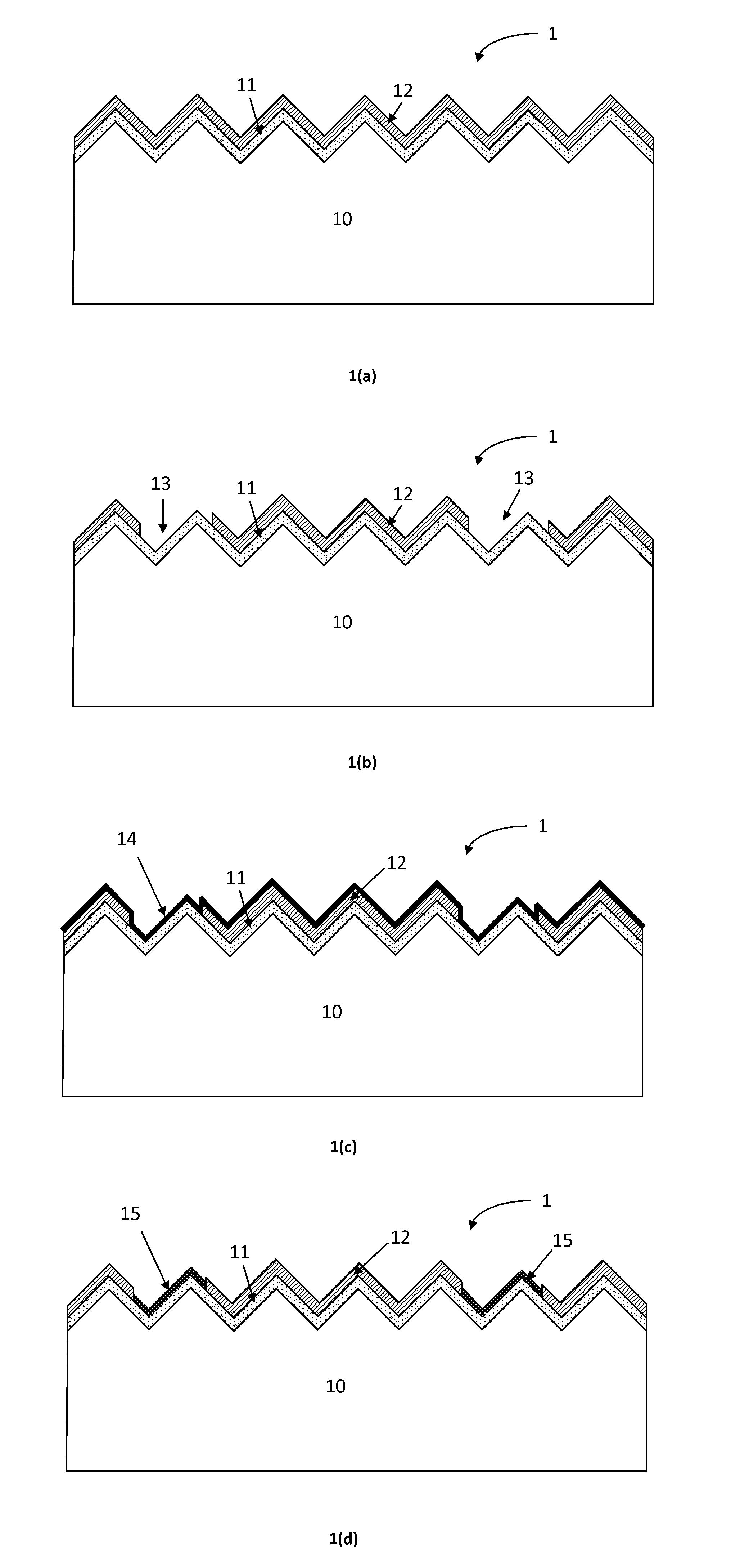
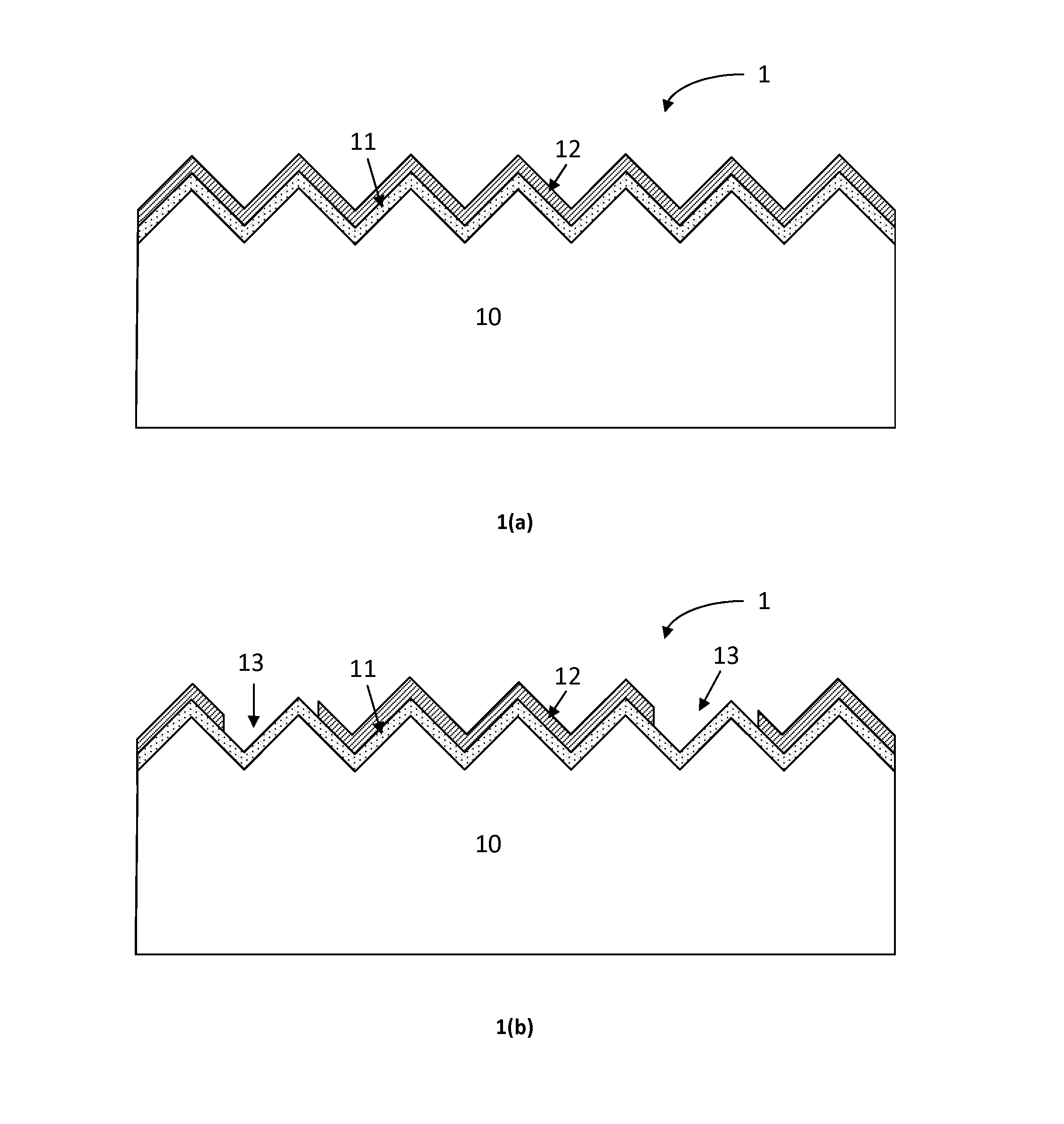
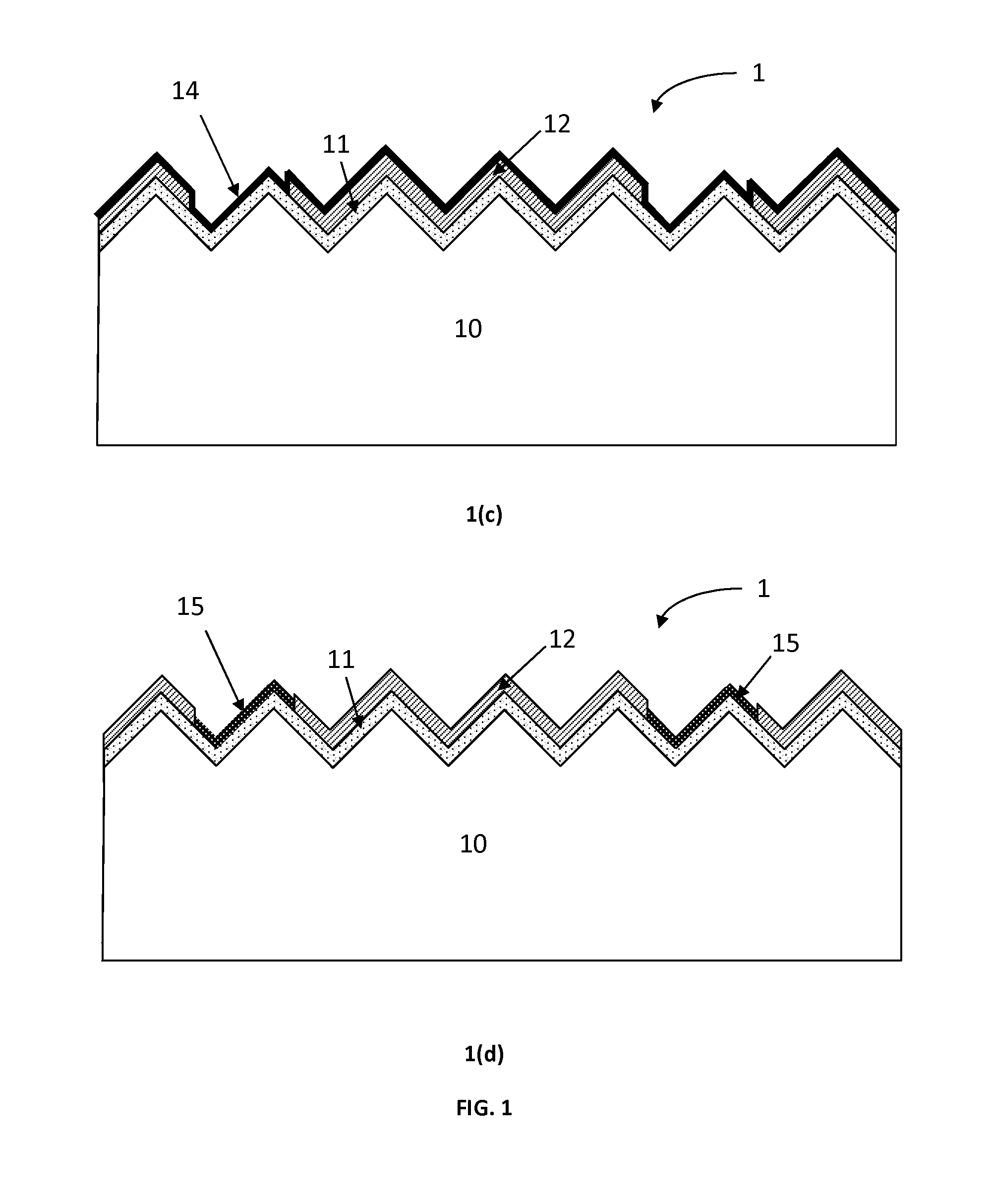
[0030]In the context of the present description, the front surface or front side of a photovoltaic cell is the surface or side adapted for being oriented towards a light source and thus for receiving illumination. The back surface, back side, rear surface or rear side of a photovoltaic cell is the surface or side opposite to the front surface. The front side of a substrate is the side of the substrate corresponding to the front side of the photovoltaic cell to be fabricated, while the rear side or back side of the substrate corresponds to the back side of the photovoltaic cell to be fabricated.

[0031]Certain embodiments relate to a method for forming a patterned metal silicide layer on a silicon substrate, the method comprising: providing a dielectric layer on the silicon substrate; forming openings through the dielectric layer at locations where a metal silicide layer needs to be formed; providing a thin metal layer comprising the metal on the substrate, at least at the location of ...


PUM

PropertyMeasurementUnit
wavelengthaaaaaaaaaa
sizeaaaaaaaaaa
thicknessaaaaaaaaaa

Abstract

The present invention is related to a method for forming a metal silicide layer on a textured silicon substrate surface. The method includes providing a metal layer on a textured silicon substrate and performing a pulsed laser annealing step providing at least one UV laser pulse with a laser fluence in the range between 0.1 J / cm2 and 1.5 J / cm2 and with a laser pulse duration in the range between 1 ns and 10 ms. Then, the method includes converting at least part of the metal layer into a metal silicide layer. In addition, the present invention is related to the use of such a method in a process for fabricating a photovoltaic cell, wherein the dielectric layer is a surface passivation layer, or wherein the dielectric layer is an antireflection coating.

Description

FIELD OF THE INVENTION[0001]The disclosed technology relates to a method of forming metal silicide layers, and more in particular, a method of forming patterned metal silicide layers in a metallization process for silicon photovoltaic cells.BACKGROUND[0002]The current industrial standard processes for front side metallization of silicon photovoltaic cells are based on printing of silver pastes or inks that need to be fired for good contact formation. Traditional screen printing of silver pastes is limited to emitters having a sheet resistance in the order of 60 to 90 Ohm / square, with an emitter surface concentration above 1020 at / cm3 to allow sufficient Ag crystallite formation.[0003]Due to their excellent contact properties, nickel silicide layers can be used for forming good contacts on lowly doped emitters with a surface concentration lower than 1020 at / cm3. Nickel silicide layers can be formed by providing a thin nickel layer (e.g. by electroless plating) on a silicon surface, f...

Claims


Application Information

Patent Timeline
Patent Type & Authority Applications(United States)
IPC IPC(8): H01L31/0236H01L21/268H01L31/0216H01L21/3205
CPCH01L31/02366H01L21/32053H01L21/268H01L31/02168H01L31/022425H01L31/1864Y02E10/50Y02P70/50
Inventor TOUS, LOICALEMAN, MONICAJOHN, JOACHIMEMERAUD, THIERRY
Owner INTERUNIVERSITAIR MICRO ELECTRONICS CENT (IMEC VZW)
Why Eureka
Try Eureka