Resistive switching memory device having improved nonlinearity and method of fabricating the same

a nonlinearity and resistive switching technology, applied in the direction of bulk negative resistance effect devices, semiconductor devices, electrical equipment, etc., can solve the problems of complex structure, difficult operation of single oxide film structure in on-state nonlinearity, and insufficient realization of nonlinearity characteristics, etc., to achieve high integration, improve on-state nonlinearity characteristics, and facilitate fabrication of cross-point rerams

Inactive Publication Date: 2014-11-20
IND ACADEMIC CORP FOUND YONSEI UNIV
View PDF5 Cites 1 Cited by
  • Summary
  • Abstract
  • Description
  • Claims
  • Application Information

AI Technical Summary

Benefits of technology

[0031]As set forth above, when the interfacial nonlinearity resistive switching memory device based on tunnel barrier engineering is developed by the method of the present invention from among a variety of methods of fabricating a nonvolatile resistive switching memory, it is possible to improve the on-state nonlinearity characteristic and develop a high-performance, high-integrated and reliable resistive switching memory device. I

Problems solved by technology

However, interference is caused by a sneak current between neighboring cells due to the unique characteristics of the cross-bar cell array, and an error occurs in a data reading operation or the like.
However, this method of the related art has the following problems: The structure is complicated since each

Method used


Image

  • Resistive switching memory device having improved nonlinearity and method of fabricating the same
  • Resistive switching memory device having improved nonlinearity and method of fabricating the same
  • Resistive switching memory device having improved nonlinearity and method of fabricating the same

Examples


examples

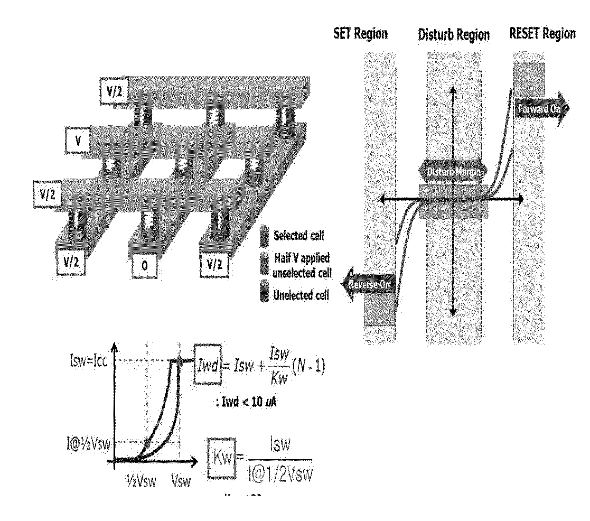
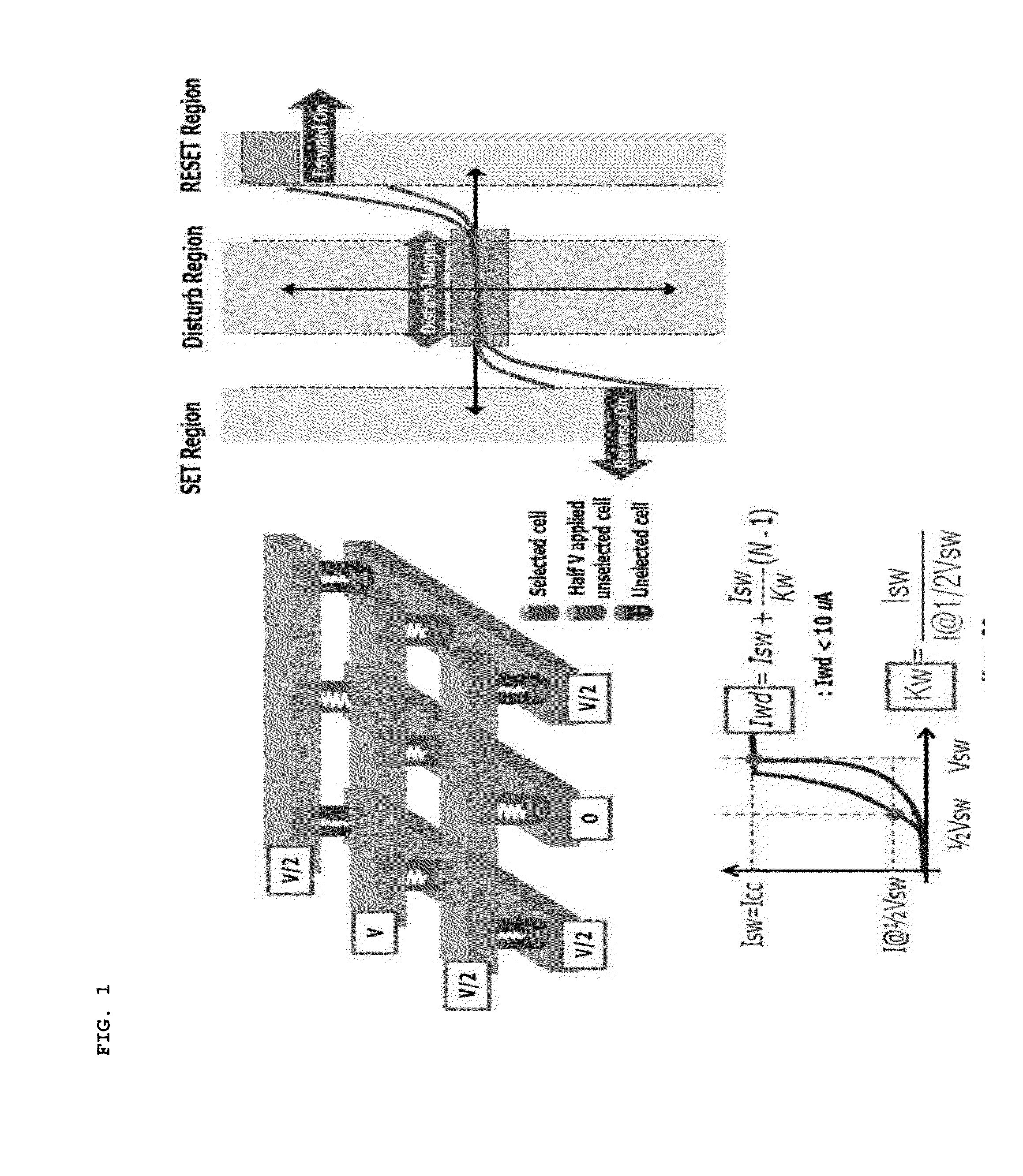
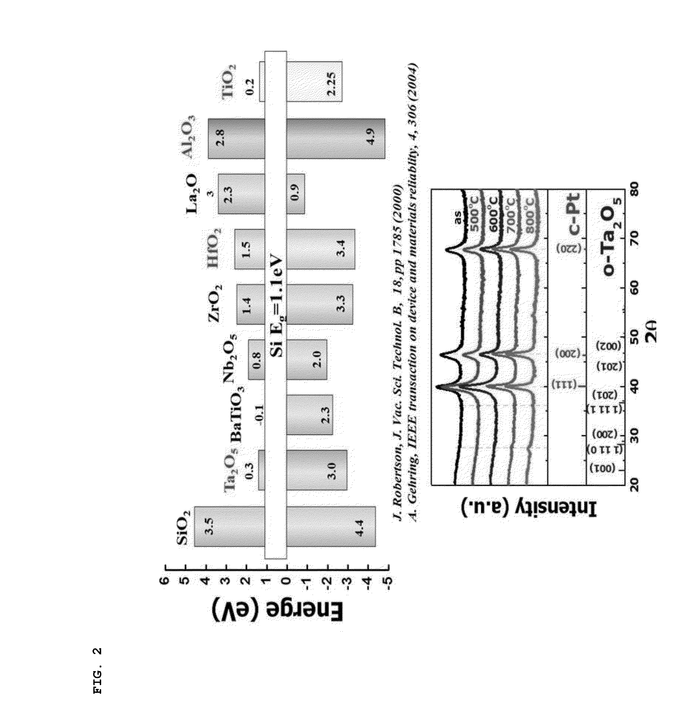
[0052]The inventors deposited different thicknesses of O3 reactant-based Ta2O5 tunnel barrier oxide films on Pt electrode-based 250×250 nm2 contact hole-type devices. Each of the tunnel barrier oxide films has a low band gap, a low conduction band offset and a crystallization temperature of 500° C. or higher, and does not cause interface switching. Afterwards, a H2O reactant-based HfO2 metal oxide film which serves for interface resistive switching was deposited, and TiN serving as the upper electrode was deposited on the metal oxide film. (In this manner, a TiN / HfO2 / Ta2O5 / Pt device was fabricated.)

[0053]As a comparative example of the present invention, an ReRAM device was formed under the same conditions except for the tunnel barrier oxide film (i.e. a TiN / HfO2 / Pt device was fabricated). In this case, a forming process is enabled when a high voltage is applied under a positive (+) external bias, and a reset process is enabled under a negative (−) external bias. However, a nonlinea...


PUM


Abstract

A nonvolatile resistive switching memory (ReRAM) device having no selection device is provided. The ReRAM device includes a lower electrode that is formed on on a substrate; a metal oxide layer that is formed on the lower electrode, the metal oxide layer having a resistive switching characteristic; an upper electrode that is formed on the metal oxide layer; and a tunnel barrier oxide film that is formed between the lower electrode and the metal oxide layer, thereby forming a double oxide film structure, the tunnel barrier oxide film being made of a material, a band energy gap and a conduction band offset of which are lower than those of the metal oxide layer, and which does not cause interface switching.

Description

CROSS REFERENCE TO RELATED APPLICATION[0001]The present application claims priority from Korean Patent Application Number 10-2013-0054287 filed on May 14, 2013, the entire contents of which are incorporated herein for all purposes by this reference.BACKGROUND OF THE INVENTION[0002]1. Field of the Invention[0003]The present invention relates to a resistive switching memory device, and more particularly, to a resistive switching memory device having improved nonlinearity characteristic and a method of fabricating the same.[0004]2. Description of Related Art[0005]The semiconductor industry has developed successfully up to the present based on miniaturization and integration in the 1980s and ultra-miniaturization and high-integration in the 1990s. These successes are based on the device operating principle that can remain unchanged even if the size of the device is reduced. Therefore, all research and development have been made on an extension from the traditional technologies, and the ...

Claims


Application Information

Patent Timeline
IPC IPC(8): H01L45/00
CPCH01L45/1608H01L45/145H10N70/801H10N70/24H10N70/883H10N70/8833H10N70/826H10N70/20H10N70/021
Inventor SOHN, HYUN CHULKO, DAE HONGKIM, JONG GIOH, JIN HOKIM, YOUNG JAE
Owner IND ACADEMIC CORP FOUND YONSEI UNIV
Why Eureka
Try Eureka