Semiconductor device and method for manufacturing same

Active Publication Date: 2014-12-04
MITSUBISHI ELECTRIC CORP
View PDF11 Cites 27 Cited by
  • Summary
  • Abstract
  • Description
  • Claims
  • Application Information

AI Technical Summary

Benefits of technology

This patent describes a semiconductor device that requires fewer photolithography and impurity implantation processes. This reduces manufacturing costs and allows for a more efficient production of the device. Additionally, the device has high breakdown voltage resistance, which is achieved by reducing the amount of impurities implanted into multiple layers.

Problems solved by technology

The application of a voltage exceeding the breakdown voltage leads to an avalanche breakdown in the portion inside the semiconductor substrate, in which an electric field is concentrated.
As a result, the depletion layer is damaged, which causes short-circuit current to flow.
Although it is this depletion layer that maintains high voltage, the breakdown voltage is limited due to an electric field concentration at the edge (peripheral edge) of the high-concentration P-type implantation layer.
The RESURF structure unfortunately has such a drawback that, in terms of high breakdown voltage resistance, an electric field is concentrated also on the peripheral edge of the RESURF layer.
In other words, increasing breakdown voltage with the use of the normal RESURF structure is limited.

Method used


Image

  • Semiconductor device and method for manufacturing same
  • Semiconductor device and method for manufacturing same
  • Semiconductor device and method for manufacturing same

Examples


first embodiment

A. First Embodiment

[0069]

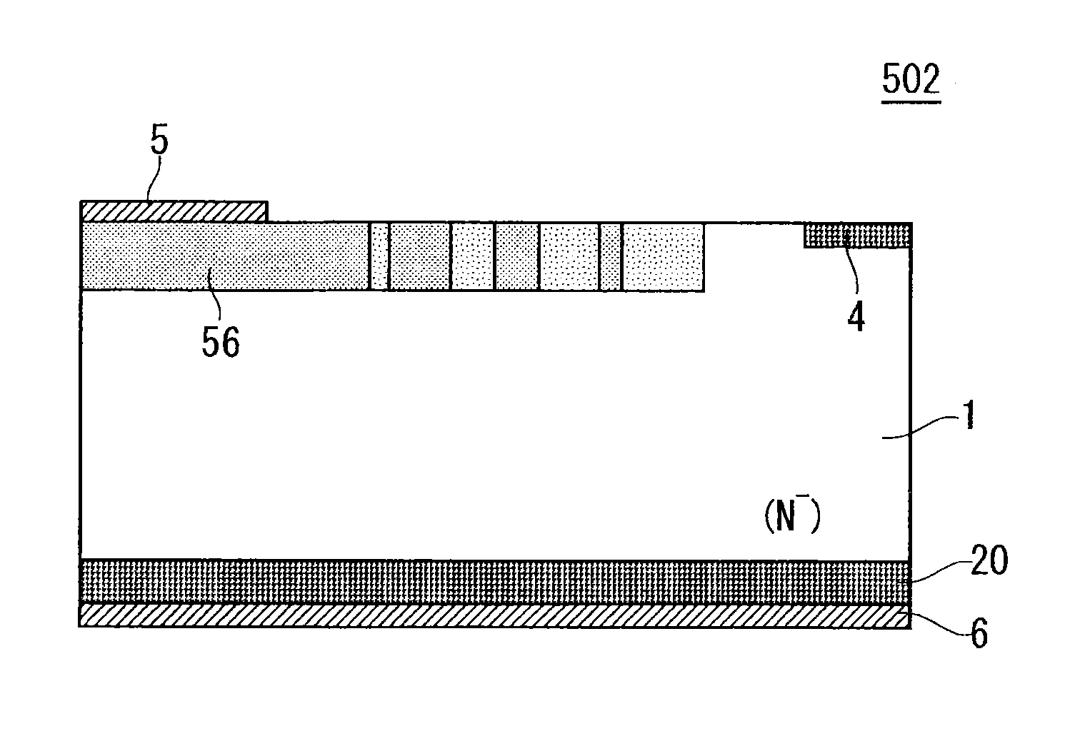
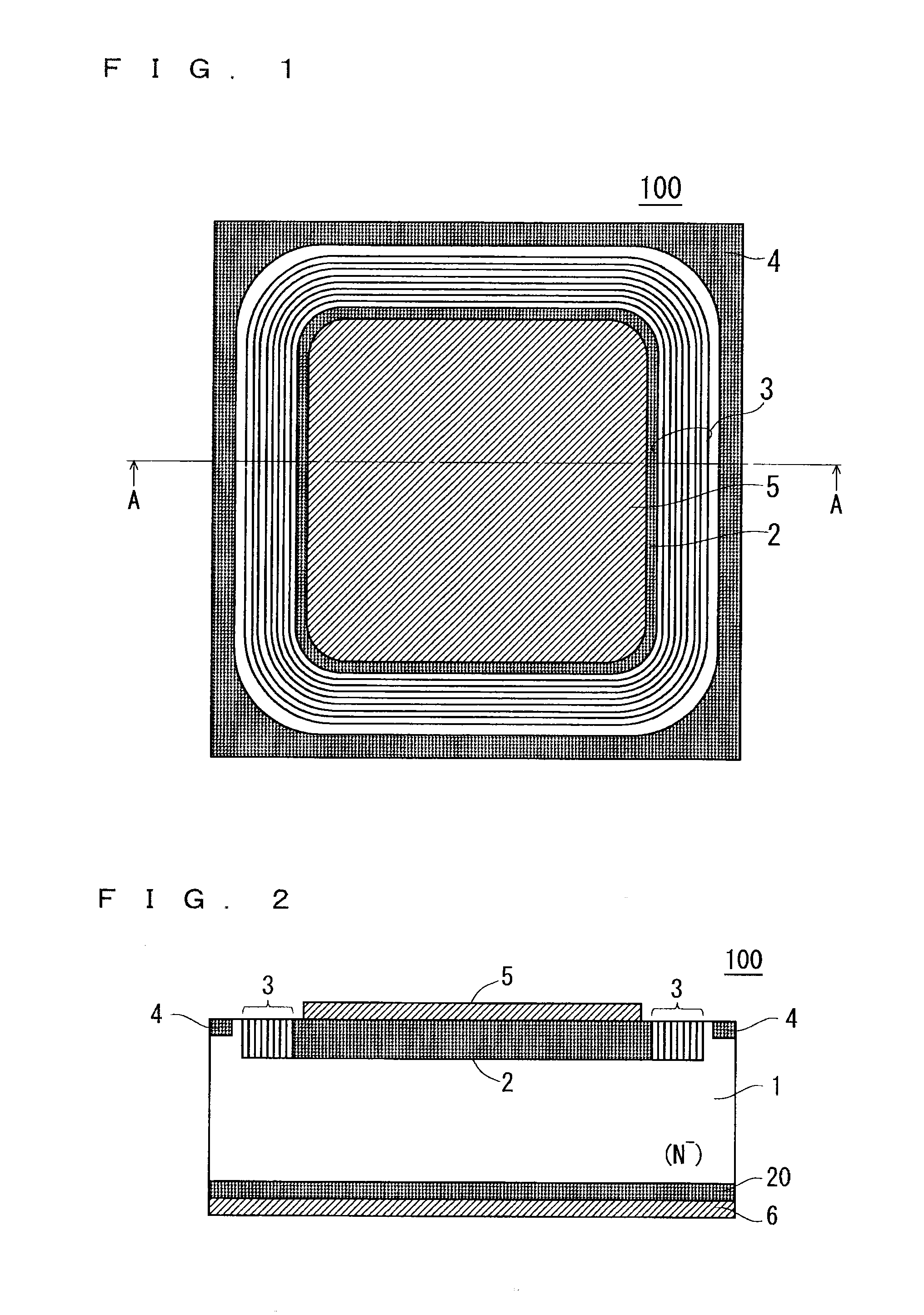
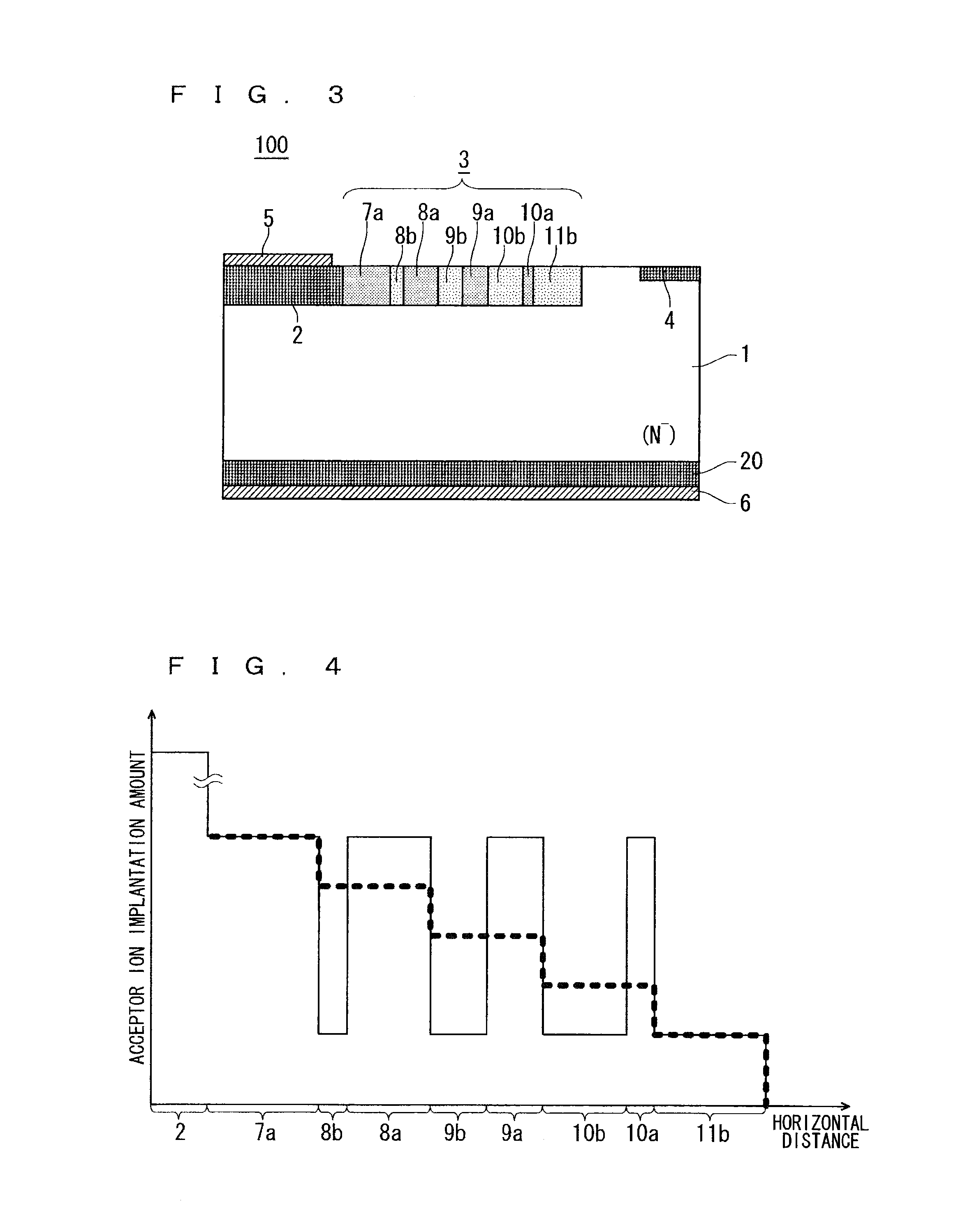
[0070]FIG. 3 is a partial cross-sectional view of the vertical PIN diode 100 to which the present invention is applied, shown in FIG. 1.

[0071]As shown in FIG. 3, the active region (P-base layer) 2 containing a relatively high concentration of P-type impurities is formed in the surface of the semiconductor substrate 1 containing a relatively low concentration (N) of N-type impurities. The P-RESURF layer 3 (electric field relaxation layer) formed of a plurality of P-type implantation layers having different concentrations is formed to surround the P-base layer 2.

[0072]The stopper layer 4 containing a relatively high concentration of N-type impurities is formed at the device edge that is located apart from the P-RESURF layer 3.

[0073]The P-RESURF layer 3 is formed of two types of P-type implantation layers having different implantation amounts. For brevity, here, the two types of P-type implantation layers have a substantially identical implantation depth and ar...

second embodiment

B. Second Embodiment

[0134]

[0135]FIG. 15 is a partial cross-sectional view showing the configuration of an N-channel type MOSFET 200 to which the present invention is applied. The MOSFET 200 is an asymmetric lateral MOSFET and is referred to as a laterally doped MOSFET (LDMOSFET).

[0136]As shown in FIG. 15, the MOSFET 200 includes an N-type implantation layer (drain layer) 22 containing a relatively high concentration of N-type impurities that is provided in the front surface of one main surface of the semiconductor substrate 21 containing a relatively low concentration (P) of P-type impurities, a P-type implantation layer (P-well layer) 26 containing a relatively high concentration of P-type impurities provided in the surface of the semiconductor substrate 21 that is located apart from the drain layer 22, an N-type implantation layer (source layer) 27 containing a relatively high concentration of N-type impurities that is provided in the upper layer portion of the P-well layer 26, an...

third embodiment

C. Third Embodiment

[0161]In the lateral MOSFET according to the second embodiment of the present invention described above, all of the N-RESURF layers need to be formed of impurity layers having the same conductivity type for causing current to flow through the breakdown voltage structure. In the vertical diode as described in the first embodiment, however, the P-RESURF layer has a termination structure, and thus, all of the P-RESURF layers need not to be formed of impurity layers having the same conductivity type. Description will be given below of an example in which the RESURF layers are formed of impurity layers having different conductivity types.

[0162]

[0163]FIG. 20 is a partial cross-sectional view showing the configuration of a PIN diode 300 in a case where the present invention is applied to a vertical diode. The same references denote the same components as those of the PIN diode 100 shown in FIG. 3, and redundant description will not be given.

[0164]A RESURF layer 31 shown ...


PUM


Abstract

A semiconductor device includes an active region formed in an upper layer portion of a semiconductor layer of a first conductivity type, and a plurality of electric field relaxation layers disposed from an edge of the active region toward the outside so as to surround the active region. The plurality of electric field relaxation layers include a plurality of first electric field relaxation layers and a plurality of second electric field relaxation layers alternately disposed adjacent to each other, the first electric field relaxation layer and the second electric field relaxation layer adjacent to each other forming a set. Impurities of a second conductivity type are implanted to the first electric field relaxation layers at a first surface density, widths of which becoming smaller as apart from the active region. Impurities of the second conductivity type are implanted to the second electric field relaxation layers at a second surface density lower than the first surface density, widths of which becoming larger as apart from the active region.

Description

TECHNICAL FIELD[0001]The present invention relates to semiconductor devices, and particularly, to a semiconductor device for power electronics that has a breakdown voltage of at least kilovolts.BACKGROUND ART[0002]Examples of the semiconductor devices (power semiconductor devices) having a breakdown voltage of 100 volts or higher that are used in power electronics include diodes, metal-oxide-semiconductor field-effect-transistors (MOSFETs), and insulated gate bipolar transistors (IGBTs). Those semiconductor devices are provided with the breakdown voltage structure for maintaining breakdown voltage resistance.[0003]For example, the semiconductor device (vertical device) that flows current perpendicularly to the main surface of the semiconductor substrate has a termination structure formed so as to surround a region (active region) functioning as an active element, which serves as the breakdown voltage structure.[0004]The semiconductor device (horizontal device) that flows current in ...

Claims


Application Information

Patent Timeline
IPC IPC(8): H01L29/06H01L29/66H01L29/861H01L29/78H01L21/266H01L29/872
CPCH01L29/063H01L21/266H01L29/872H01L29/66659H01L29/7835H01L29/66136H01L29/66143H01L29/8611H01L29/0615H01L29/0619H01L29/0847H01L29/42368H01L29/1608H01L29/0692H01L29/0638
Inventor KAWAKAMI, TSUYOSHIHAMADA, KENJIEBIHARA, KOHEIFURUKAWA, AKIHIKOMURAKAMI, YUJI
Owner MITSUBISHI ELECTRIC CORP
Why Eureka
Try Eureka