Microwave emission mechanism, microwave plasma source and surface wave plasma processing apparatus

a plasma processing apparatus and microwave plasma technology, applied in plasma techniques, electric discharge tubes, nano-devices, etc., can solve the problems of difficult to uniformly perform plasma processing on a scaled-up semiconductor wafer at a high speed, inflicting plasma damage on a micro-device, etc., and achieve the effect of increasing the plasma density

Active Publication Date: 2014-12-11
TOKYO ELECTRON LTD
View PDF2 Cites 123 Cited by
  • Summary
  • Abstract
  • Description
  • Claims
  • Application Information

AI Technical Summary

Benefits of technology

[0010]In view of the above, the present invention provides a microwave emission mechanism, a microwave plasma source and a surface wa...

Problems solved by technology

However, in a parallel plate type plasma processing apparatus or an inductively coupled plasma processing apparatus which has been conventionally used, an electron temperature of a generated plasma is high, so that...

Method used


Image

  • Microwave emission mechanism, microwave plasma source and surface wave plasma processing apparatus
  • Microwave emission mechanism, microwave plasma source and surface wave plasma processing apparatus
  • Microwave emission mechanism, microwave plasma source and surface wave plasma processing apparatus

Examples


Embodiment Construction

[0027]Hereinafter, embodiments of the present invention will be described in detail with reference to the accompanying drawings.

[0028](Configuration of Surface Wave Plasma Processing Apparatus)

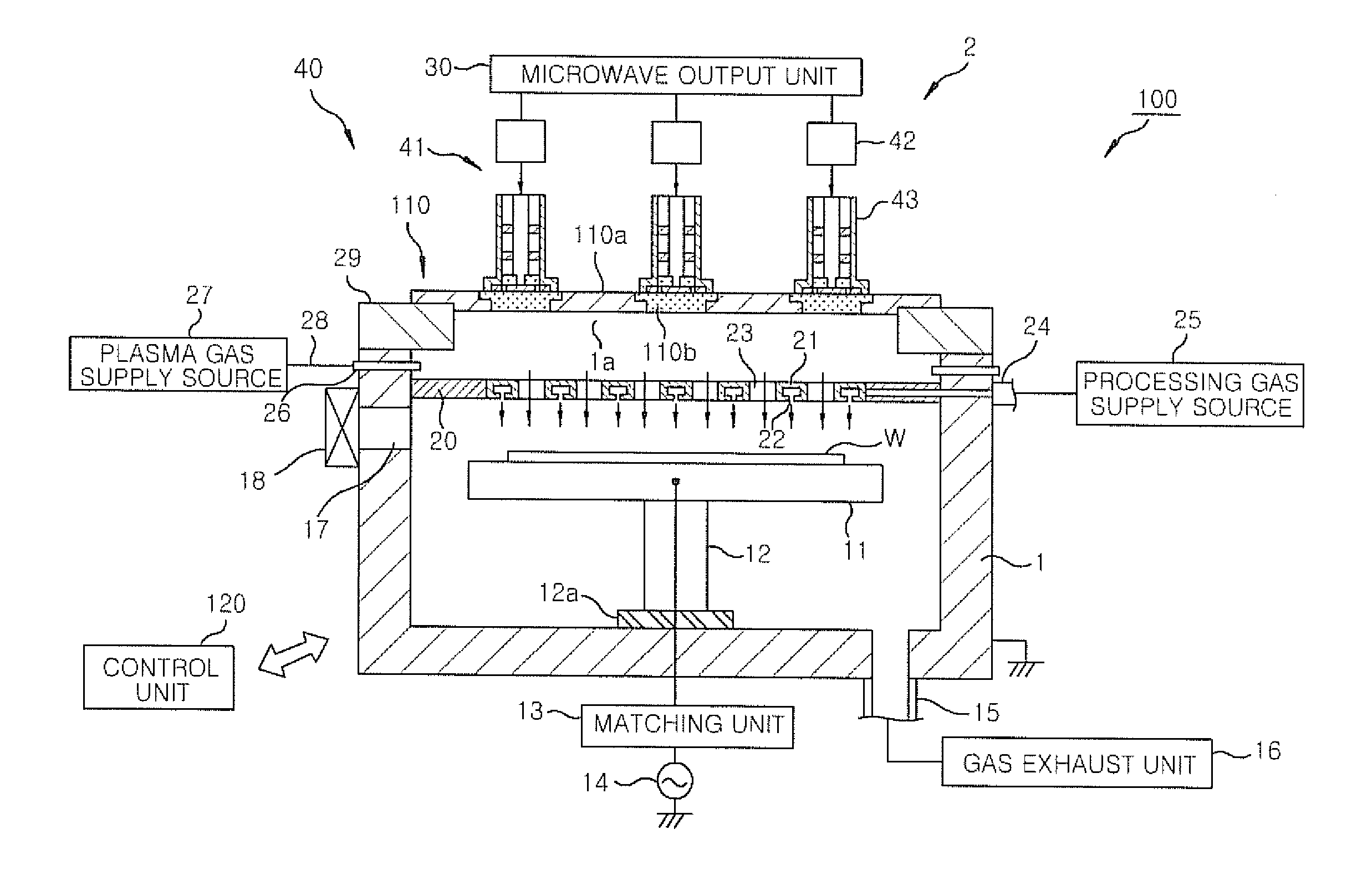
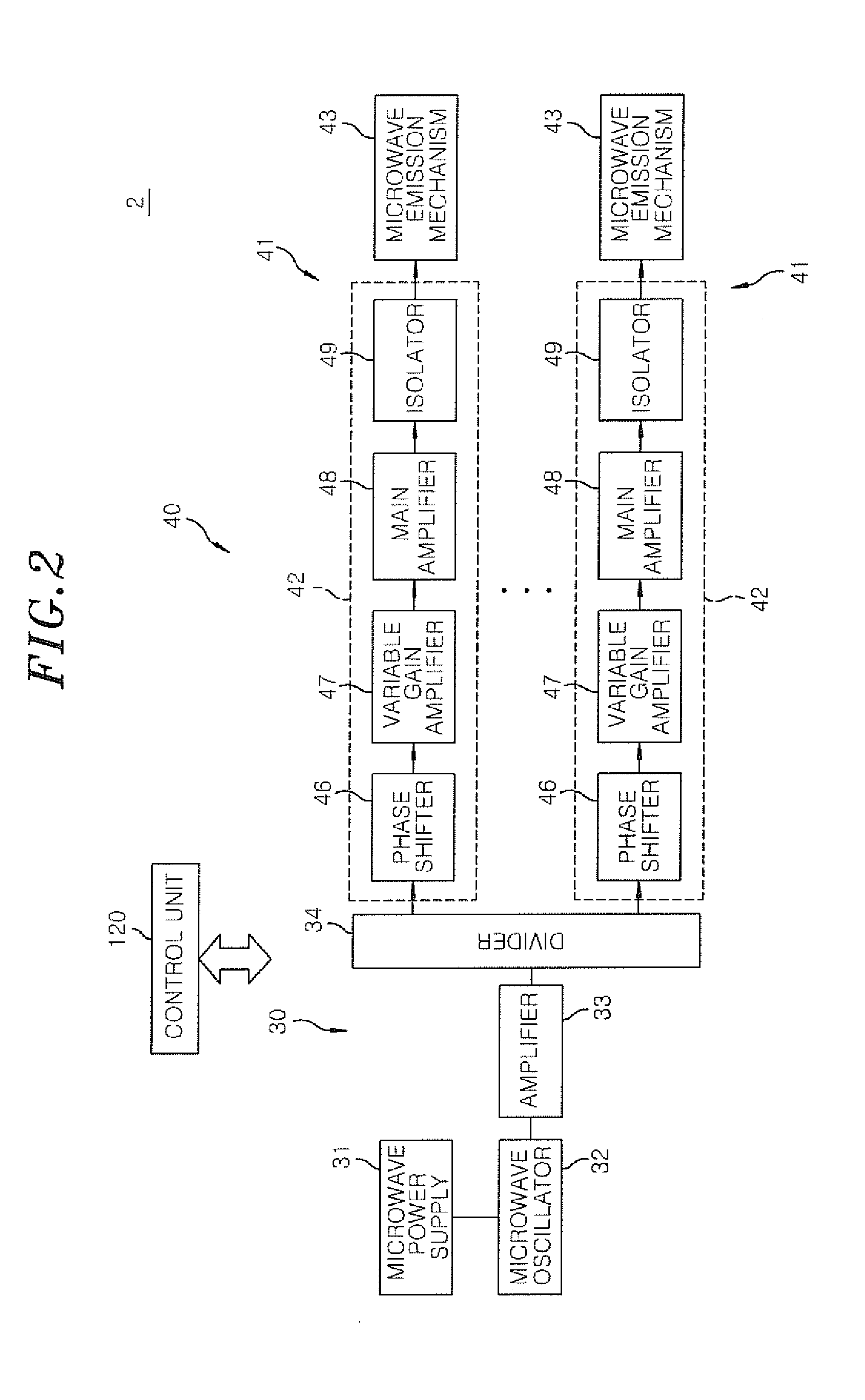
[0029]FIG. 1 is a cross sectional view showing a schematic configuration of a surface wave plasma processing apparatus including a microwave emission mechanism in accordance with an embodiment of the present invention. FIG. 2 shows a configuration of a microwave plasma source for use in the surface wave plasma processing apparatus shown in FIG. 1. FIG. 3 is a top view schematically showing a microwave supply unit in the microwave plasma source.

[0030]The surface wave plasma processing apparatus 100 is configured as a plasma etching apparatus for performing a plasma process, e.g., an etching process, on a wafer. The surface wave plasma processing apparatus 100 includes: a substantially cylindrical airtight chamber 1 which is grounded and made of a metallic material such as aluminum, stainless st...


PUM


Abstract

A microwave emission mechanism includes: a transmission path through which a microwave is transmitted; and an antenna section that emits into a chamber the microwave transmitted through the transmission path. The antenna section includes an antenna having a slot through which the microwave is emitted, a dielectric member through which the microwave emitted from the antenna is transmitted and a closed circuit in which a surface current and a displacement current flow. A surface wave is formed in a surface of the dielectric member. The closed circuit has at least: an inner wall of the slot; and the surface and an inner portion of the dielectric member. When a wavelength of the microwave is λ0, a length of the closed circuit is nλ0±δ, where n is a positive integer and δ is a fine-tuning component including 0.

Description

FIELD OF THE INVENTION[0001]The present invention relates to a microwave emission mechanism, a microwave plasma source and a surface wave plasma processing apparatus.BACKGROUND OF THE INVENTION[0002]Plasma processing is a necessary technology in manufacturing a semiconductor device. Along with the recent demand for high integration and high speed of an LSI (Large Scale Integration), a design rule of the semiconductor device forming the LSI requires miniaturization and a semiconductor wafer becomes scaled up. Accordingly, a plasma processing apparatus is required to respond to such miniaturization and scaling up.[0003]However, in a parallel plate type plasma processing apparatus or an inductively coupled plasma processing apparatus which has been conventionally used, an electron temperature of a generated plasma is high, so that plasma damage is inflicted on a micro-device. Further, since a high-density plasma region is locally distributed, it is difficult to uniformly perform plasma...

Claims


Application Information

Patent Timeline
IPC IPC(8): H01J37/32
CPCH01J37/32266H01J37/32229H01J37/3222H01J37/32201H01J37/32192H01J37/3244H05H1/46H05H1/4615H05H1/463H05H1/4622
Inventor IKEDA, TAROMIYASHITA, HIROYUKIOSADA, YUKIFUJINO, YUTAKAKOMATSU, TOMOHITO
Owner TOKYO ELECTRON LTD
Why Eureka
Try Eureka