Electro-optic device, method of manufacturing electro-optic device, and electronic apparatus

a manufacturing method and electrooptic technology, applied in the direction of solid-state devices, semiconductor devices, thermoelectric devices, etc., can solve the problems of difficult to completely block the influence of moisture, and cracks are more likely to be generated in inorganic compound films. , to achieve the effect of reducing the influence of stress on segmentation along the segmentation lin

Active Publication Date: 2014-12-18
SEIKO EPSON CORP
View PDF7 Cites 27 Cited by
  • Summary
  • Abstract
  • Description
  • Claims
  • Application Information

AI Technical Summary

Benefits of technology

[0012]Since the outer edge of the first inorganic sealing layer is disposed so as to be separated from the segmentation lines, the influence of stress that advances an initial crack of the segmentation line is decreased, and thus a defect (crack or the like) is less likely to be generated in the first inorganic sealing layer due to the stress. Accordingly, the infiltration of moisture and oxygen into the light emitting element through the defect of the first inorganic sealing layer is suppressed, and the deterioration of the light emitting element due to the moisture and the oxygen is suppressed. Therefore, it is possible to improve long-term reliability of the electro-optic device.Application Example 2
[0018]The outer edge of the second inorganic sealing layer is disposed more than 0.1 mm away from the end face, and thus it is possible to suppress the influence of the plane defect and the line defect which are generated in the first surface of the substrate when segmenting the mother substrate. That is, it is possible to make it harder for a defect to be generated in the second inorganic sealing layer due to the plane defect and the line defect which are generated in the first surface of the substrate when segmenting the mother substrate.Application Example 5
[0035]The planarization layer is constituted by any one of a metal oxide formed of polysilazane or formed by a sol-gel method and an epoxy resin. The metal oxide and the epoxy resin have a dense film structure as compared with, for example, a hydrocarbon system polymer such as polyethylene, polystyrene, or polypropylene, and have an excellent barrier property against moisture and oxygen. The planarization layer is constituted by the metal oxide or the epoxy resin, and thus it is possible to improve the barrier property against moisture and oxygen as compared with a case where the planarization layer is constituted by a hydrocarbon system polymer.Application Example 13
[0039]The electronic apparatus according to this application example includes the electro-optic device according to the above-described application example. In the electro-optic device, the deterioration of the light emitting element is suppressed by the planarization layer and the first inorganic sealing layer, and long-term reliability is excellent. For example, the electro-optic device according to the above-described application example is applied to a display unit of an electronic apparatus such as a head mounted display, a digital camera, a personal computer, a portable information terminal, a navigator, a viewer, or a head-up display, and thus it is possible to realize a stable display that is excellent in long-term reliability.Application Example 15
[0043]In the method of manufacturing the electro-optic device according to this application example, in a state where the first inorganic sealing layer suppressing the deterioration of the light emitting element is formed in each of the plurality of electro-optic devices disposed in the mother substrate so as to be more than 0.1 mm away from the segmentation lines, the mother substrate is segmented along the segmentation lines to form the simplex electro-optic devices. Since the first inorganic sealing layer is more than 0.1 mm away from the segmentation line, the influence of stress exerted for the segmentation along the segmentation lines is decreased, and thus a defect is less likely to be generated in the first inorganic sealing layer due to the stress.

Problems solved by technology

However, the method of JP-A-2004-119138 has a problem that it is difficult to completely block the influence of moisture.
The silicon oxynitride or the silicon oxide constituting the inorganic compound film is less flexible than, for example, the epoxy resin constituting the thermosetting resin, and thus a crack is likely to be generated due to stress or strain (deformation).
When the mother substrate is divided along the segmentation lines, stress or strain is inevitably applied to the multilayer film or the sealing film near the segmentation lines, and thus a crack is more likely to be generated in the inorganic compound film constituting the multilayer film or the sealing film.
There is a concern that moisture may infiltrate into the organic EL element through the crack, depending on a state of the crack.
Further, when the organic EL device is used for a long time, external stress such as heat or pressure is applied to the organic EL device, and thus the crack generated at the time of segmenting the mother substrate increases in size (grows), which leads to a concern that moisture may infiltrate into the organic EL element.
That is, there is a problem of long-term reliability being deteriorated.

Method used


Image

  • Electro-optic device, method of manufacturing electro-optic device, and electronic apparatus
  • Electro-optic device, method of manufacturing electro-optic device, and electronic apparatus
  • Electro-optic device, method of manufacturing electro-optic device, and electronic apparatus

Examples


first embodiment

Outline of Organic EL Device

[0064]An organic EL device 100 according to a first embodiment is an example of an electro-optic device, displays a monochrome image, and can be suitably used in a display unit such as a head mounted display (HMD) to be described later or a digital camera.

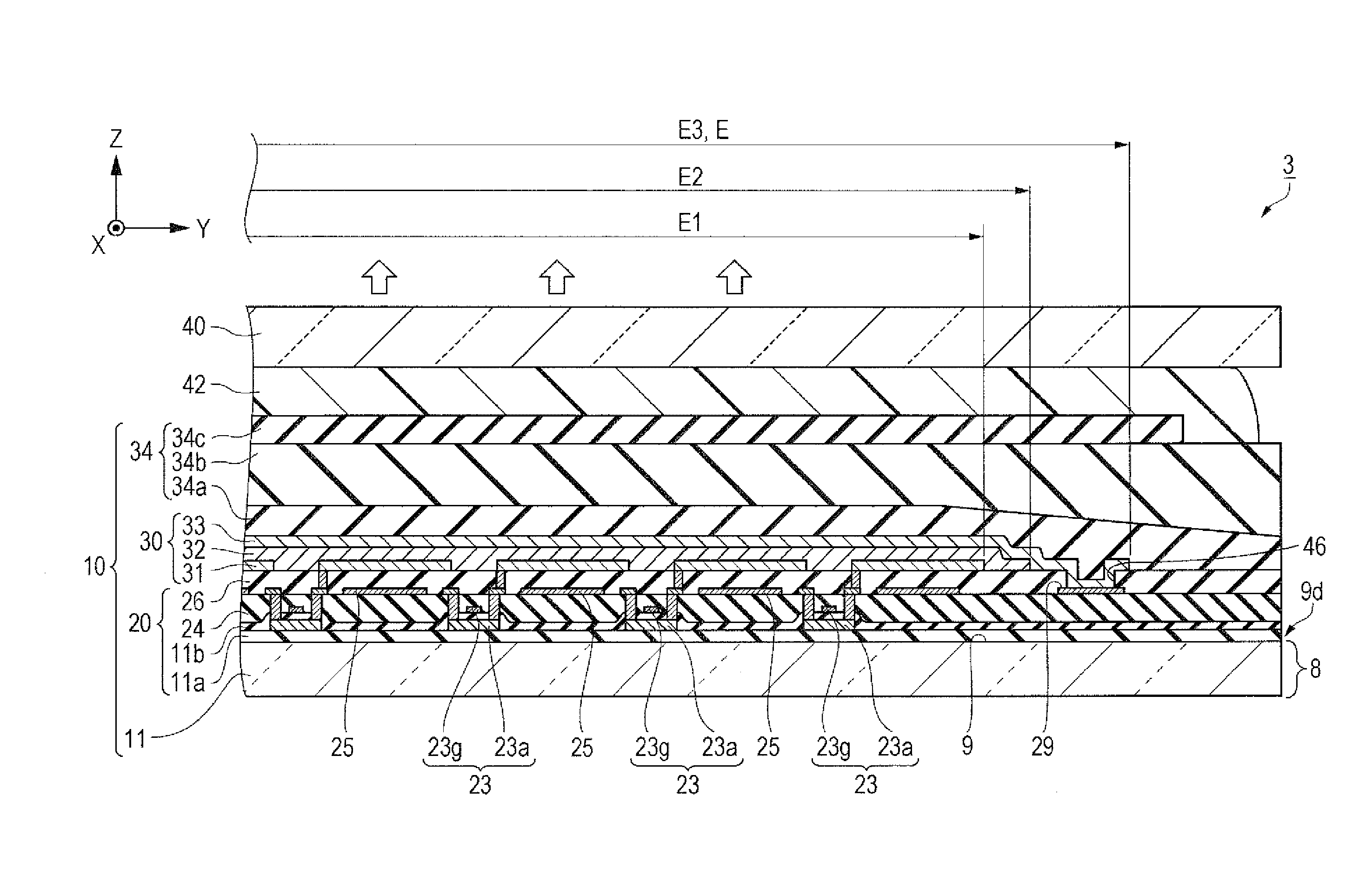
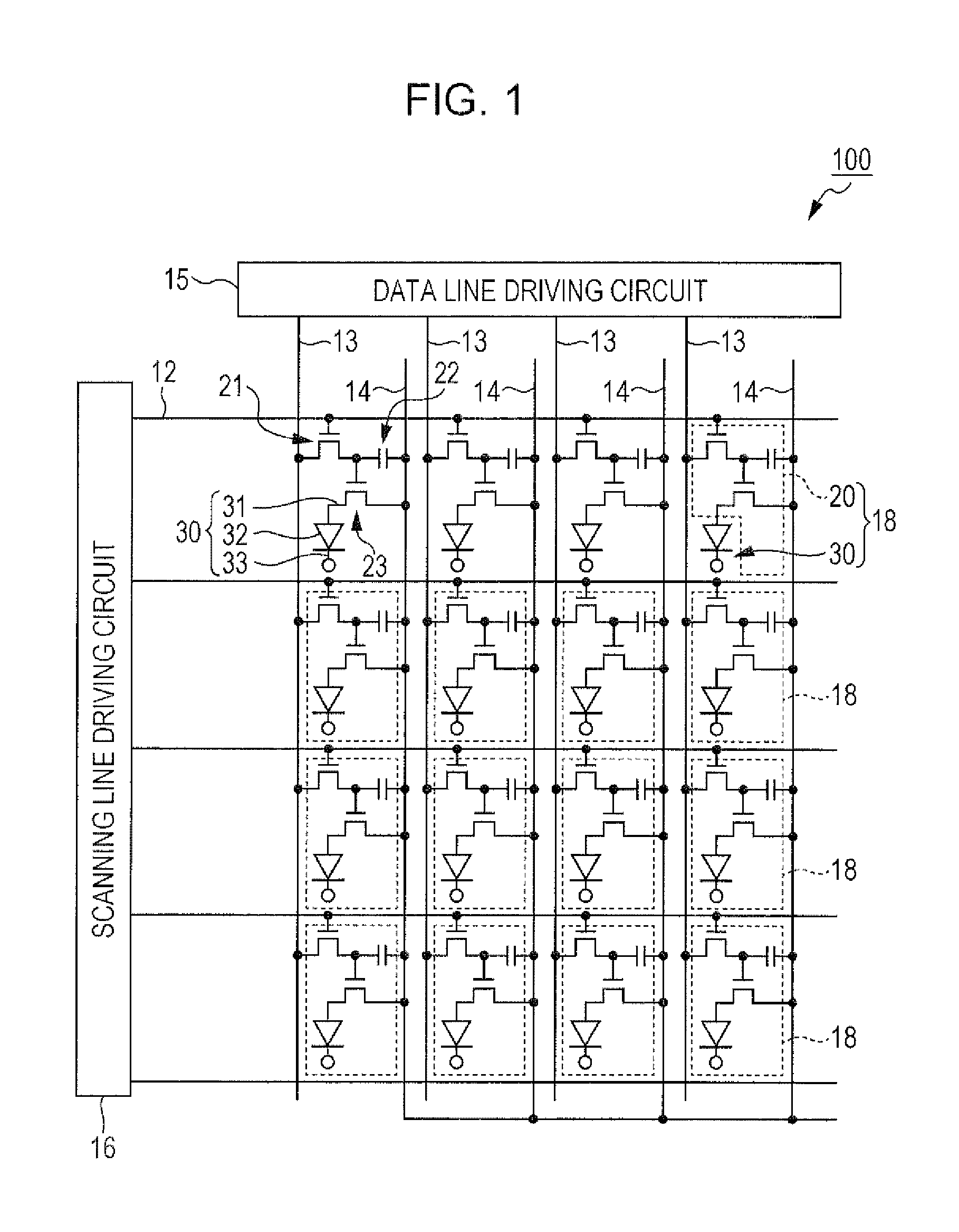
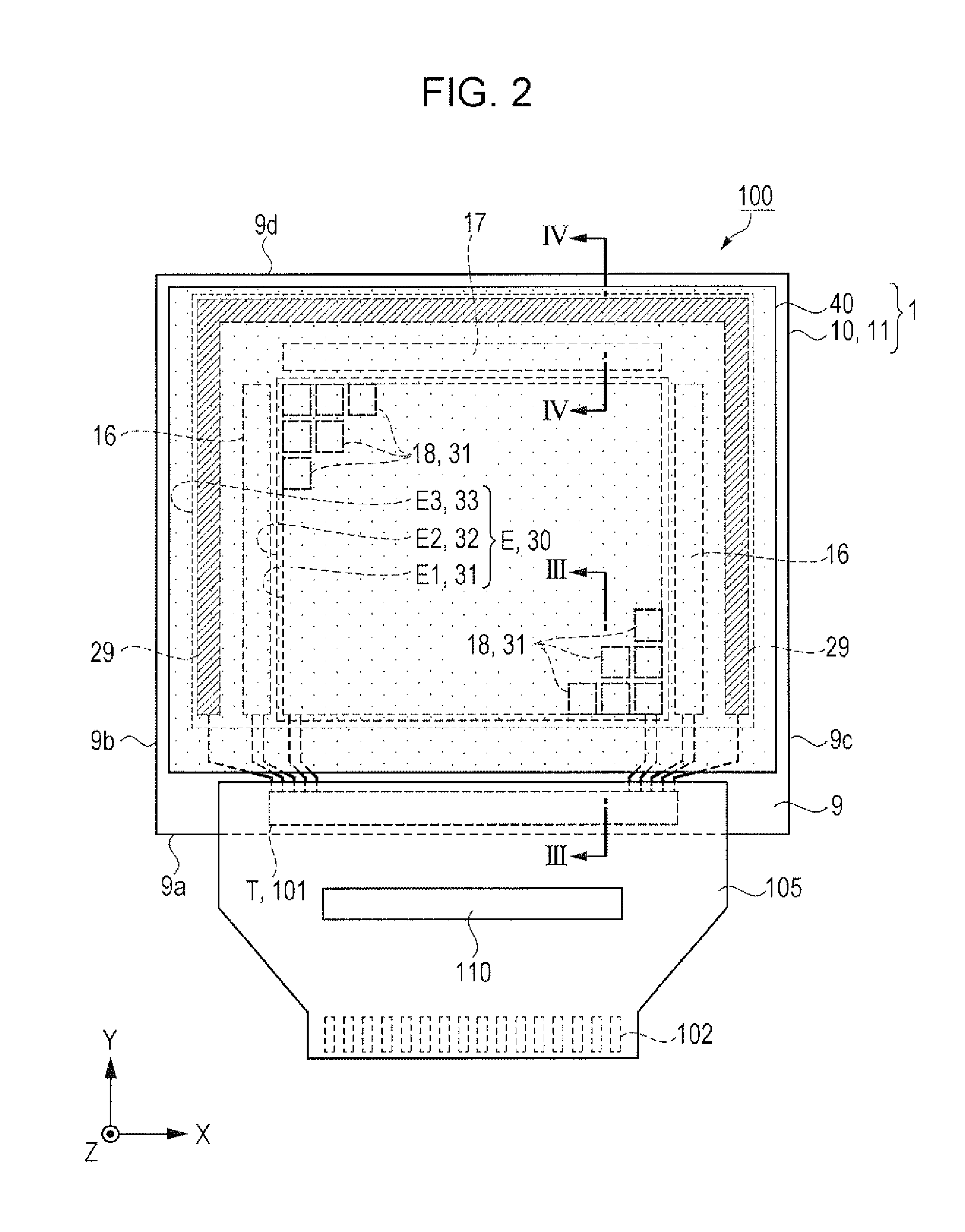
[0065]First, an outline of the organic EL device 100 according to this embodiment will be described with reference to FIGS. 1 and 2. FIG. 1 is an equivalent circuit diagram showing the electrical configuration of the organic EL device according to this embodiment. FIG. 2 is a schematic plan view showing the configuration of the organic EL device according to this embodiment.

[0066]As shown in FIG. 1, the organic EL device 100 according to this embodiment includes a plurality of scanning lines 12 and a plurality of data lines 13 which cross each other, and a plurality of power lines 14 which are arrayed in parallel with the respective plurality of data lines 13. The scanning lines 12 are connected to a sca...

second embodiment

Outline of Organic EL Device

[0163]FIG. 10 is a schematic plan view showing the configuration of an organic EL device according to a second embodiment. FIG. 11 is a schematic cross-sectional view showing the structure of the organic EL panel taken along line XI-XI (green (G) colored layer) of FIG. 10. FIG. 12 is a schematic cross-sectional view showing the structure of the organic EL panel taken along line XII-XII (region in which a green colored layer is disposed) of FIG. 10. FIG. 13 is a schematic plan view of a terminal region.

[0164]Hereinafter, an organic EL device 200 according to this embodiment will be described with reference to FIGS. 10 to 13 focusing on the differences from the first embodiment. In addition, the same components as those in the first embodiment will be denoted by the same reference numerals, and repeated description will be omitted.

[0165]The main differences between this embodiment and the first embodiment are that the organic EL device 200 (an organic EL pa...

third embodiment

[0180]FIG. 14 corresponds to FIG. 2 and is a schematic plan view of an organic EL device according to a third embodiment. FIG. 15 corresponds to FIG. 4 and is a schematic cross-sectional view showing the structure of the organic EL panel taken along line XV-XV of FIG. 14.

[0181]Hereinafter, an organic EL device 300 according to this embodiment will be described with reference to FIGS. 14 and 15 focusing on the differences from the first embodiment. In addition, the same components as those in the first embodiment will be denoted by the same reference numerals, and repeated description will be omitted.

[0182]In the organic EL device 300 according to this embodiment, the shape (size) of a protection substrate 40 is different from that in the first embodiment, and other configurations are the same as those in the first embodiment.

[0183]In the first embodiment, the protection substrate 40 is attached to each of the plurality of element substrates 10 using a method of attaching the simplex...


PUM


Abstract

An electro-optic device includes a substrate that has a first surface and an end face crossing the first surface; a light emitting element that is disposed on the first surface; a planarization layer that covers the light emitting element; and a first inorganic sealing layer that is disposed on the planarization layer. An outer edge of the first inorganic sealing layer is disposed between an outer edge of the planarization layer and a first region where the light emitting element is disposed.

Description

BACKGROUND[0001]1. Technical Field[0002]The present invention relates to an electro-optic device, a method of manufacturing the electro-optic device, and an electronic apparatus equipped with the electro-optic device.[0003]2. Related Art[0004]Organic electroluminescence (EL) devices, which are examples of electro-optic devices, are self-emitting display devices, have advantages in a reduction in thickness and weight because a backlight as a light source is not necessary as compared with, for example, a non-emission type display device such as a liquid crystal device, and are expected to be applied as micro displays which are applied to an electronic view finder or the like. The organic EL device includes an organic EL element as a light emitting element, and the organic EL element is constituted by an anode, a cathode, a light emitting functional layer interposed between the anode and the cathode, and the like. The light emitting functional layer deteriorates due to oxygen, moisture...

Claims


Application Information

Patent Timeline
Patent Type & Authority Applications(United States)
IPC IPC(8): H01L51/52H01L51/00H01L51/50H01L51/56
CPCH01L51/5256H01L51/5012H01L51/0024H01L51/56H10K59/38H10K59/131H10K50/841H10K50/8426H10K50/8445H10K50/844H10K71/851
Inventor AKAGAWA, SUGURUFUKAGAWA, TAKEFUMI
Owner SEIKO EPSON CORP
Why Eureka
Try Eureka