Semiconductor device

a technology of semiconductor devices and semiconductors, applied in semiconductor devices, semiconductor/solid-state device details, electrical apparatus, etc., can solve problems such as peeling or drop-off, etching failure, etc., and achieve the effects of reducing film thickness, reducing leak current, and improving electrical properties

Active Publication Date: 2015-01-22
TOYODA GOSEI CO LTD
View PDF6 Cites 7 Cited by
  • Summary
  • Abstract
  • Description
  • Claims
  • Application Information

AI Technical Summary

Benefits of technology

[0017]According to any of the aspects of the invention described above, the first layer serves to reduce the leak current on the interface of the semiconductor layer, whereas the second layer serves to reinforce the dielectric breakdown strength and thereby reduce the film thickness required for the first layer. This accordingly achieves both improvement of the electrical properties and improvement of the workability of the protective film.

Problems solved by technology

Increasing the thickness of the protective film made of A2O3 to ensure the sufficient dielectric breakdown strength, however, causes a problem of etching failure (peel-off or drop-off of a resist mask) during processing by wet etching.

Method used


Image

  • Semiconductor device
  • Semiconductor device
  • Semiconductor device

Examples


first embodiment

A. First Embodiment

[0026]A-1. Configuration of Semiconductor Device

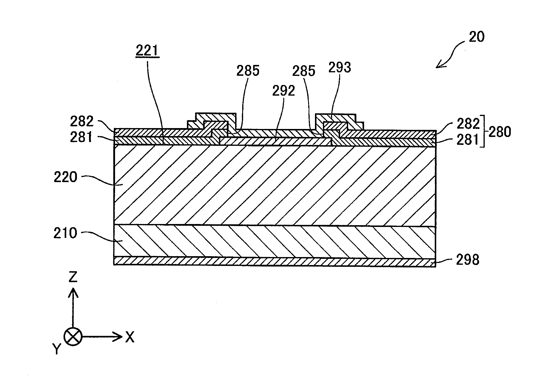
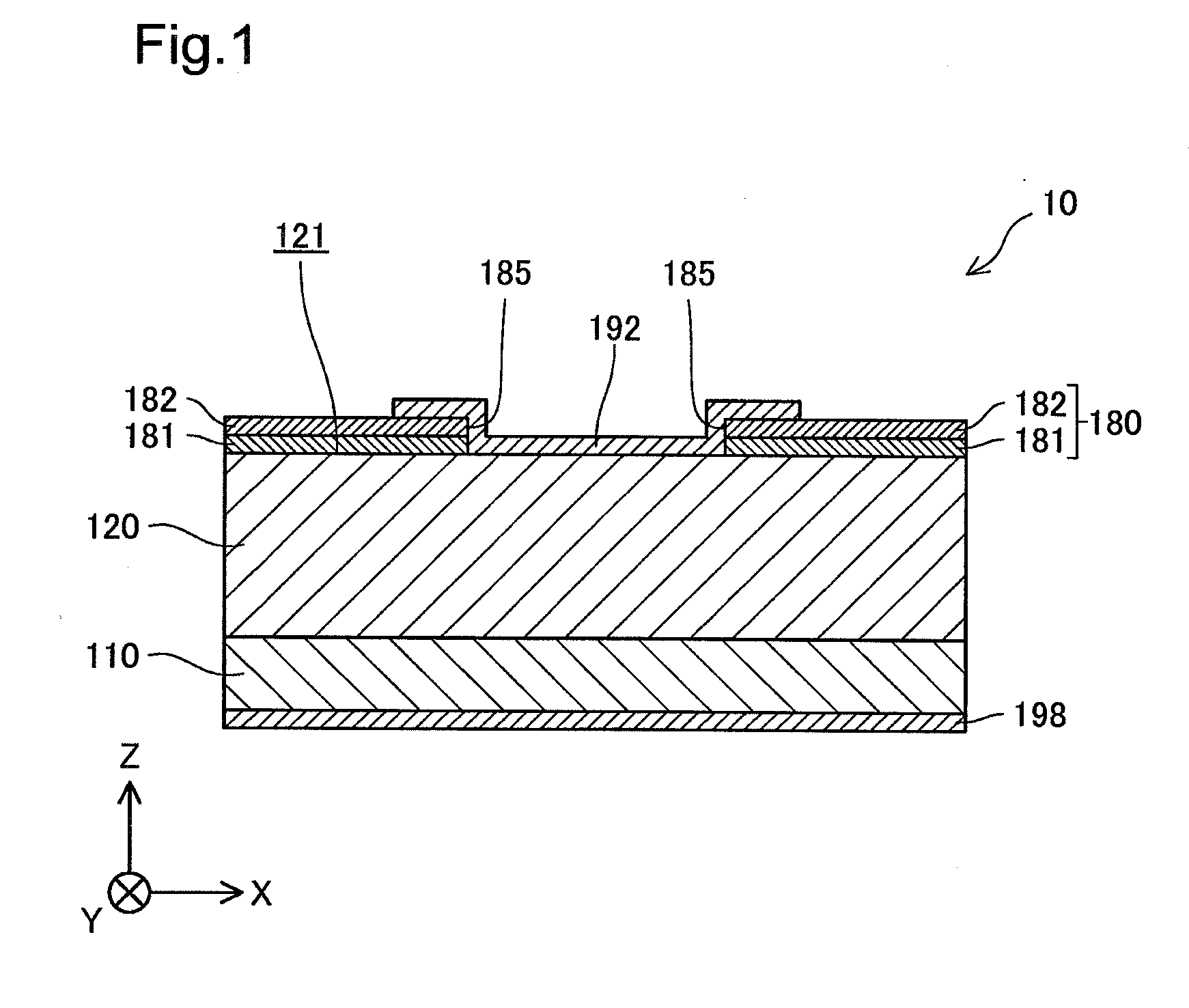
[0027]FIG. 1 is a cross sectional view schematically illustrating the configuration of a semiconductor device 10 according to a first embodiment. X, Y and Z axes orthogonal to one another are shown in FIG. 1.

[0028]Among the XYZ axes shown in FIG. 1, the X axis is an axis from the left side of the sheet surface to the right side of the sheet surface; +X-axis direction represents a direction toward the right side of the sheet surface; and −X-axis direction represents a direction toward the left side of the sheet surface. Among the XYZ axes shown in FIG. 1, the Y axis is an axis from the front side of the sheet surface to the back side of the sheet surface; +Y axis direction represents a direction toward the back side of the sheet surface; and −Y-axis direction represents a direction toward the front side of the sheet surface. Among the XYZ axes shown in FIG. 1, the Z axis is an axis from the bottom of the sheet surface...

second embodiment

B. Second Embodiment

[0057]B-1. Configuration of Semiconductor Device

[0058]FIG. 4 is a cross sectional view schematically illustrating the configuration of a semiconductor device 20 according to a second embodiment. The X, Y and Z axes are also shown in FIG. 4, like FIG. 1.

[0059]The semiconductor device 20 is a GaN-based semiconductor device. According to this embodiment, the semiconductor device 20 is a vertical Schottky barrier diode. The configuration of the semiconductor device 20 of the second embodiment is similar to the configuration of the semiconductor device 10 of the first embodiment, except the configuration of a protective film and a Schottky electrode. The semiconductor device 20 includes a substrate 210, a semiconductor layer 220, a protective film 280, a Schottky electrode 292, a field plate electrode 293 and a back electrode 298.

[0060]The substrate 210 of the semiconductor device 20 is similar to the substrate 110 of the first embodiment. The semiconductor layer 220 ...


PUM


Abstract

A semiconductor device includes; a semiconductor layer mainly made of GaN; a protective film provided to have electrical insulation property and configured to coat the semiconductor layer; and an electrode provided to have electrical conductivity and configured to form a Schottky junction with the semiconductor layer. Tthe protective film includes: a first layer made of Al2O3 and arranged adjacent to the semiconductor layer; a second layer made of an electrical insulation material different from Al2O3 and formed on the first layer; and an opening structure formed to pass through the first layer and the second layer. The electrode is located inside of the opening structure.

Description

CROSS-REFERENCE TO RELATED APPLICATION[0001]The present application claims priority from Japanese patent application P2013-148168 filed on Jul. 17, 2013, the entirety of disclosures of which is hereby incorporated by reference into this application.BACKGROUND[0002]1. Technical Field[0003]The present invention relates to a semiconductor device.[0004]2. Related Art[0005]GaN-based semiconductor devices having one or more semiconductor layers mainly made of gallium nitride (GaN) have been known as one type of semiconductor devices (semiconductor elements). Some of the GaN-based semiconductor devices may serve as a Schottky barrier diode. In order to reduce the leak current on the interface of the semiconductor layer, relieve the potential crowding on the semiconductor layer and protect a junction surface between two semiconductor layers, a protective film is formed to coat the semiconductor layer in the GaN-based semiconductor device. The protective film is made of an electrical insulat...

Claims


Application Information

Patent Timeline
Patent Type & Authority Applications(United States)
IPC IPC(8): H01L23/31H01L29/47H01L29/20
CPCH01L23/3171H01L29/475H01L29/2003H01L23/3192H01L29/872H01L2924/0002H01L29/402H01L2924/00
Inventor UENO, YUKIHISAOKA, TORUHASEGAWA, KAZUYA
Owner TOYODA GOSEI CO LTD
Why Eureka
Try Eureka