Epitaxial block layer for a fin field effect transistor device

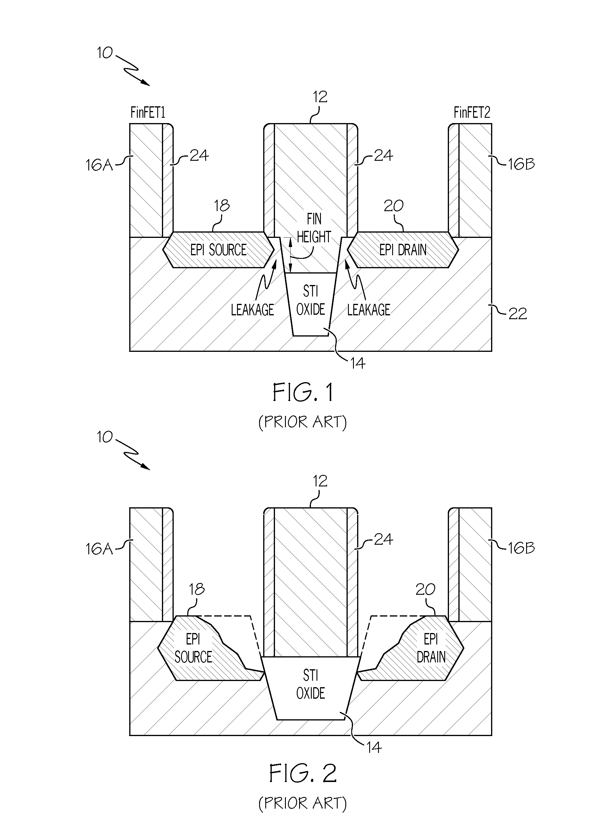
a technology of fin field effect transistor and epitaxial block layer, which is applied in the field of epitaxial block layer, can solve the problems of asymmetric growth without ideal facets, difficult patterning isolation trench b>14/b> to reach the small critical dimension (cd) required, and difficult to deplete the channel underneath the gate electrode voltage, etc., and achieves uniform epitaxial growth and epitaxial growth. uniform

Active Publication Date: 2015-01-22
GLOBALFOUNDRIES US INC
View PDF6 Cites 50 Cited by
  • Summary
  • Abstract
  • Description
  • Claims
  • Application Information

AI Technical Summary

Benefits of technology

[0009]In general, approaches for enabling uniform epitaxial (epi) growth in an epi junction area of a semiconductor device (e.g., a fin field effect transistor device) are provided. Specifically, a semiconductor device is provided including a dummy gate and a set of fin field effect transistors (FinFETs) formed over a substrate; a spacer layer formed over the dummy gate and each of the set of FinFETs; and an epi material formed within a set of recesses in the substrate, the set of recesses formed prior to removal of an epi block layer over the dummy gate.
[0010]One aspect of the present invention includes a method for forming a device, the method comprising: forming a set of fin field effect transistors (FinFETs) over a substrate; forming a spacer layer over each of the set of FinFETs; forming an epitaxial (epi) block layer over one of the FinFETs; removing a portion of the spacer layer in an epi junction area adjacent the one of the FinFETs; forming a set of recesses in the substrate in the epi junction area adjacent the one of the FinFETs; and forming an epi material within the set of recesses.
[0011]Anot

Problems solved by technology

Such effects make it harder for the voltage on a gate electrode to deplete the channel underneath and stop the flow of carriers through the channel—in other words, to turn the transistor off.
However, when the device is switched on, the gate shape limits the current through the gate to a low level.
However, patterning isolation trench 14 to reach the small critical dimensions (CD) required is difficult with conventional lithography and etch techniques available.
Furthermore, as shown in FIG. 2, dur

Method used


Image

  • Epitaxial block layer for a fin field effect transistor device
  • Epitaxial block layer for a fin field effect transistor device
  • Epitaxial block layer for a fin field effect transistor device

Examples


Embodiment Construction

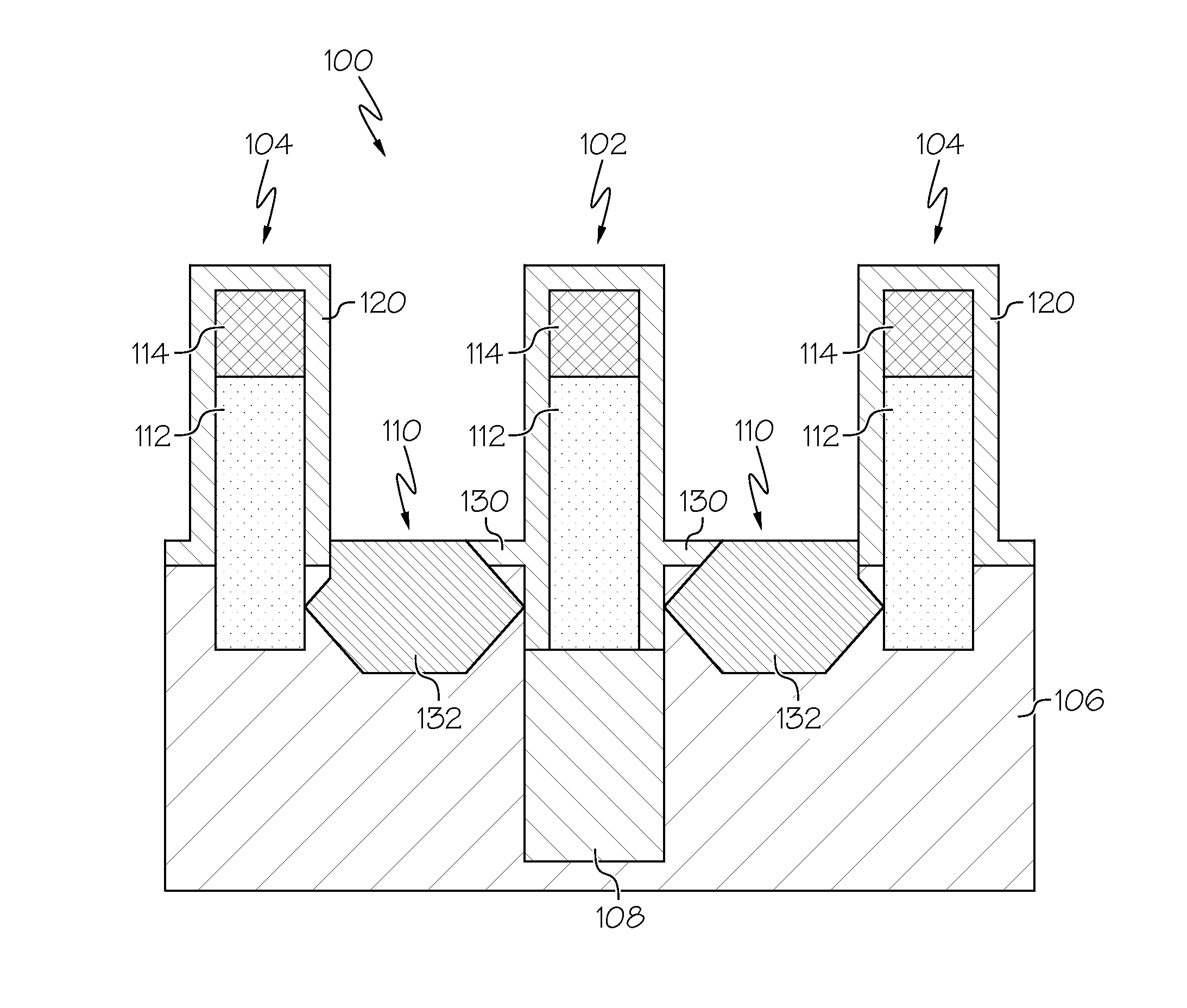
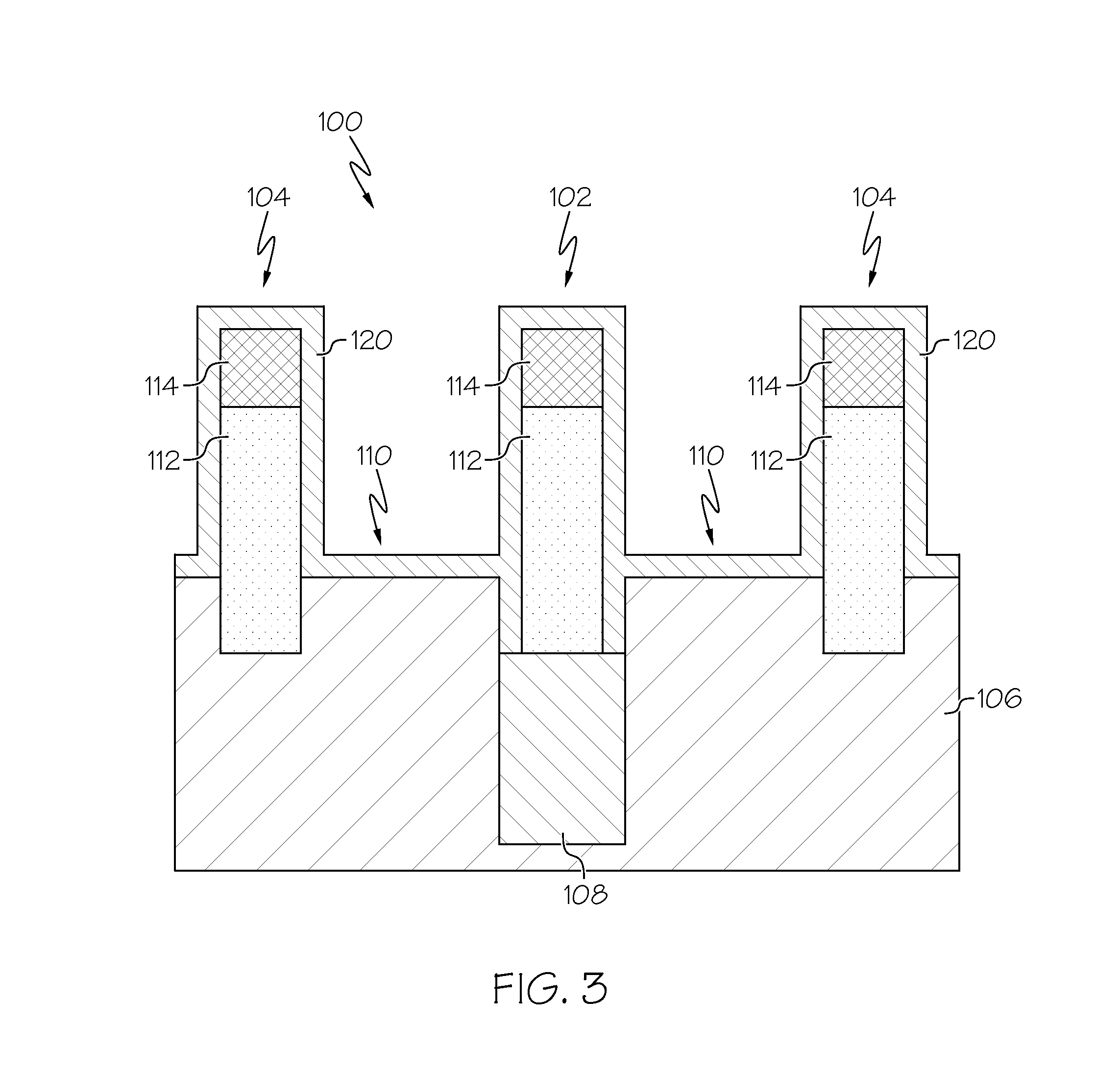
[0022]Exemplary embodiments will now be described more fully herein with reference to the accompanying drawings, in which exemplary embodiments are shown. Described are approaches for enabling uniform epitaxial (epi) growth in an epi junction area of a semiconductor device (e.g., a fin field effect transistor device). Specifically, a semiconductor device is provided including a dummy gate and a set of fin field effect transistors (FinFETs) formed over a substrate; a spacer layer formed over the dummy gate and each of the set of FinFETs; and an epi material formed within a set of recesses in the substrate, the set of recesses formed prior to removal of an epi block layer over the dummy gate.

[0023]It will be appreciated that this disclosure may be embodied in many different forms and should not be construed as limited to the exemplary embodiments set forth herein. Rather, these exemplary embodiments are provided so that this disclosure will be thorough and complete and will fully conv...


PUM


Abstract

Approaches for enabling uniform epitaxial (epi) growth in an epi junction area of a semiconductor device (e.g., a fin field effect transistor device) are provided. Specifically, a semiconductor device is provided including a dummy gate and a set of fin field effect transistors (FinFETs) formed over a substrate; a spacer layer formed over the dummy gate and each of the set of FinFETs; and an epi material formed within a set of recesses in the substrate, the set of recesses formed prior to removal of an epi block layer over the dummy gate.

Description

BACKGROUND[0001]1. Technical Field[0002]This invention relates generally to the field of semiconductors, and more particularly, to forming an epitaxial (epi) block layer to increase uniformity during epi growth in a fin field effect transistor (FinFET) device.[0003]2. Related Art[0004]A typical integrated circuit (IC) chip includes a stack of several levels or sequentially formed layers of shapes. Each layer is stacked or overlaid on a prior layer and patterned to form the shapes that define devices (e.g., field effect transistors (FETs)) and connect the devices into circuits. In a typical state of the art complementary insulated gate FET process, such as what is normally referred to as CMOS, layers are formed on a wafer to form the devices on a surface of the wafer. Further, the surface may be the surface of a silicon layer on a silicon on insulator (SOI) wafer. A simple FET is formed by the intersection of two shapes, a gate layer rectangle on a silicon island formed from the sili...

Claims


Application Information

Patent Timeline
IPC IPC(8): H01L29/78H01L29/66H01L21/02
CPCH01L29/6681H01L21/02532H01L29/785H01L21/02658H01L21/0262H01L29/66795H01L29/0653H01L29/0847H01L29/161H01L29/24H01L29/66545H01L29/66636H01L29/7848
Inventor HU, ZHENYUCARTER, RICHARD J.WEI, ANDYZHANG, QIMURALIDHARAN, SRUTHICHILD, AMY L.
Owner GLOBALFOUNDRIES US INC
Why Eureka
Try Eureka