Novel method for electromigration and adhesion using two selective deposition

a selective deposition and electromigration technology, applied in the field of semiconductor technology, can solve the problems of a substantial drop in the electrical properties of the semiconductor device, increase in electromigration, etc., and achieve the effects of preventing electromigration, improving adhesion, and effectively preventing interlayer delamination

Active Publication Date: 2015-01-29
SEMICON MFG INT (SHANGHAI) CORP
View PDF7 Cites 17 Cited by
  • Summary
  • Abstract
  • Description
  • Claims
  • Application Information

AI Technical Summary

Benefits of technology

[0024]According to the present invention, a stack of cobalt layer and an AlN layer deposited in sequence on the copper layer in the copper interconnect structure can effectively prevent electromigration caused by interlayer diffusion of the copper layer into the upper dielectric layer, and significantly improve the adhesion between that copper layer and the upper etch stop layer subsequently formed thereon, and effectively prevent the interlayer delamination.

Problems solved by technology

Due to the low mechanical strength of low dielectric constant materials and the poor adhesion between the copper and the etch stop layers disposed in the copper interconnect structure, the etch stop layer and the copper layer in the copper interconnect structure is prone to delamination that results in a diffusion of copper into the interlayer dielectric layer, thereby causing an increase in electromigration and a substantial drop in electrical properties of the semiconductor device.

Method used


Image

  • Novel method for electromigration and adhesion using two selective deposition
  • Novel method for electromigration and adhesion using two selective deposition
  • Novel method for electromigration and adhesion using two selective deposition

Examples


Embodiment Construction

[0029]Specific embodiments are described below. Those skilled in the art with access to the present disclosure will recognize that modifications and alternatives can also be implemented within the scope of the claimed invention.

[0030]The following description is of the best-contemplated mode of carrying out the invention. This description is made for the purpose of illustrating the general principles of the invention and should not be taken in a limiting sense. The scope of the invention is best determined by reference to the appended claims.

[0031]It is understood that, in this specification, the terms “comprises”, “comprising”, “includes”, “including” or similar terms may include a list of stated features, integers, steps, operations, elements, and / or components, but may also include other features, integers, steps, operations, elements, components, or any of their combinations not listed.

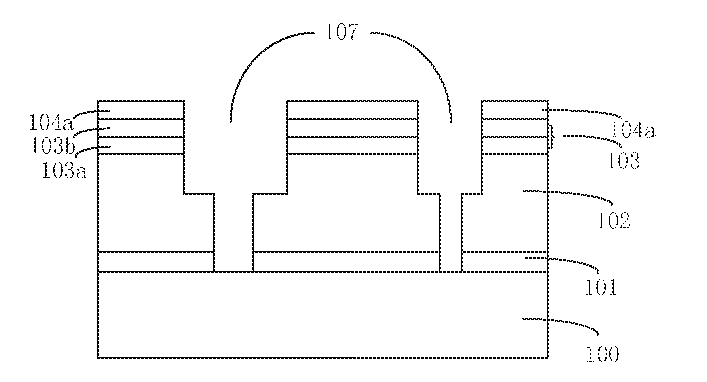
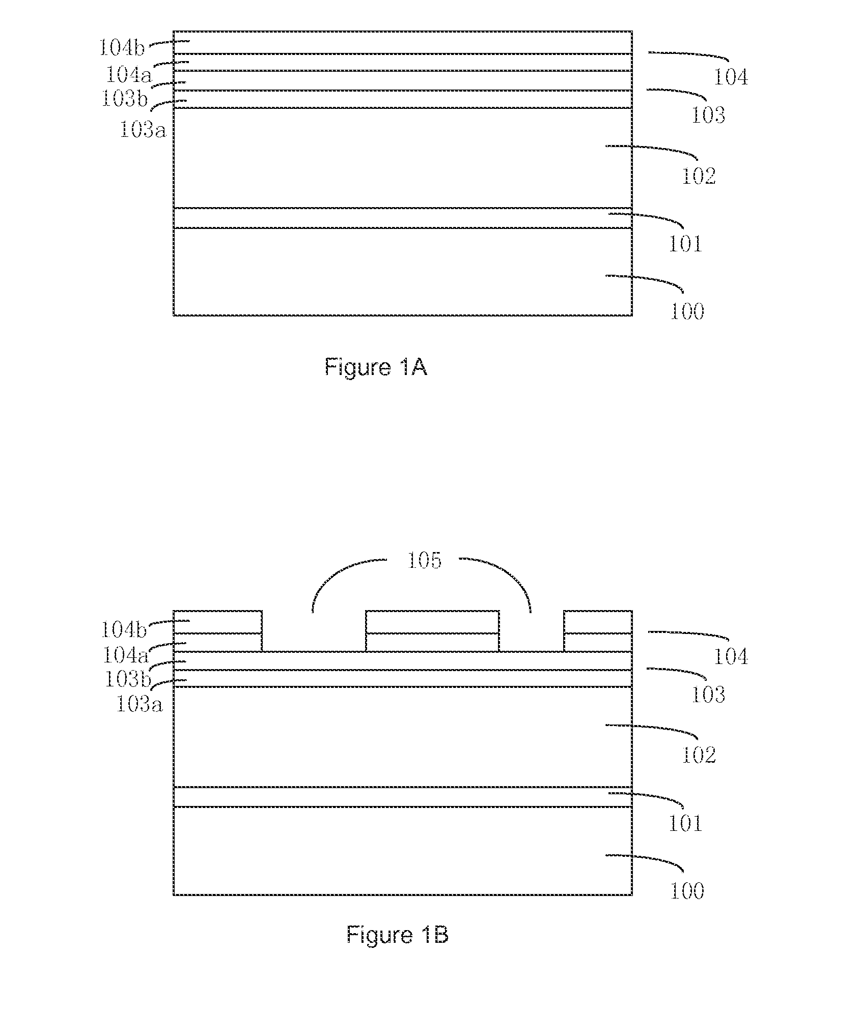
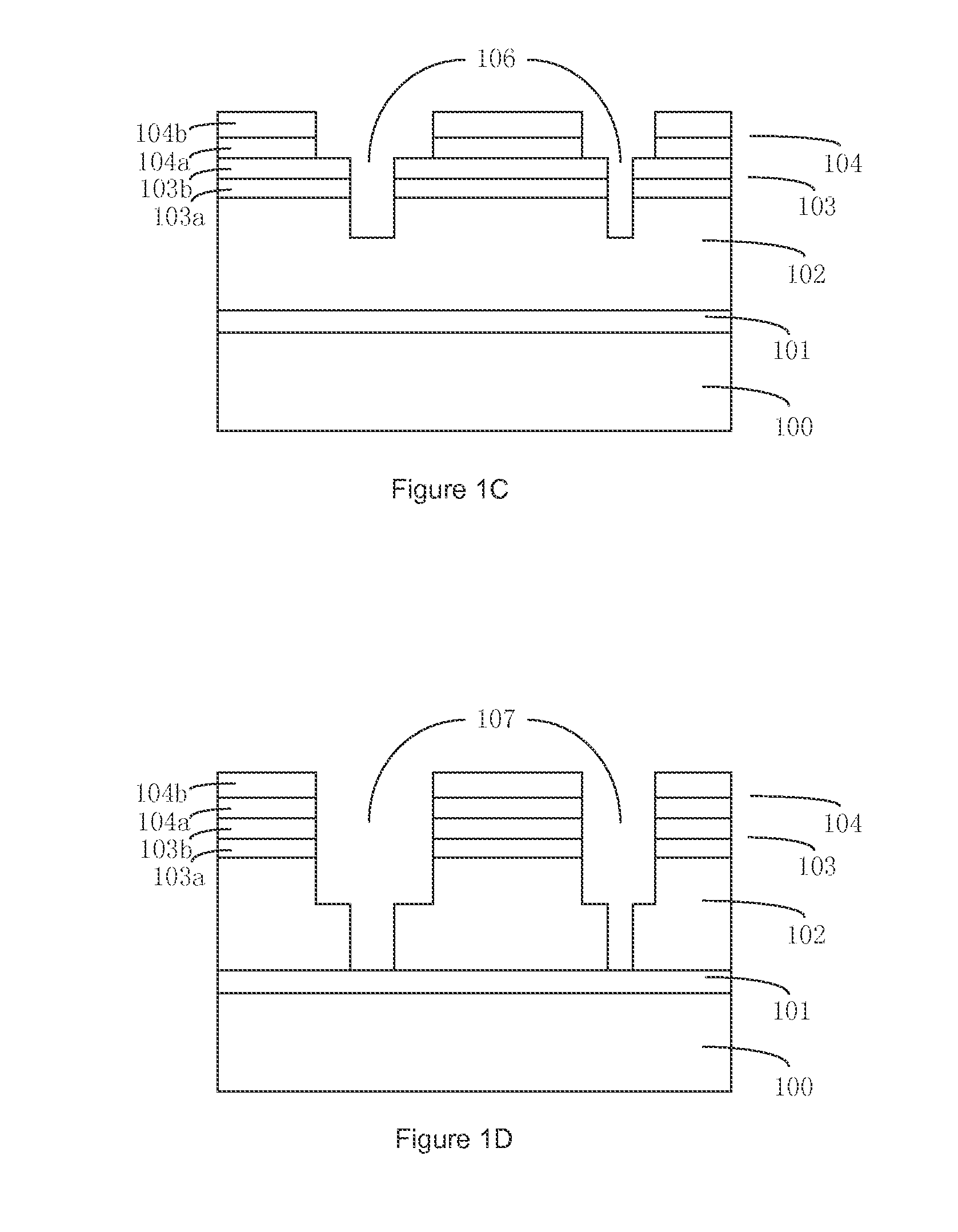
[0032]With reference to FIGS. 1A-1J and 2, process steps of a method for making a semiconducto...


PUM

PropertyMeasurementUnit
thicknessaaaaaaaaaa
pressureaaaaaaaaaa
pressureaaaaaaaaaa

Abstract

A method of manufacturing a semiconductor device includes providing a semiconductor substrate, sequentially forming an etch stop layer and an interlayer dielectric layer on the semiconductor substrate, forming a copper metal interconnect structure in the interlayer dielectric layer, forming a copper layer in the copper metal interconnect structure, forming a cobalt layer on the copper layer, and forming an aluminum nitride layer on the cobalt layer. The stack of cobalt layer and copper layer effectively suppresses electromigration caused by diffusion of the copper layer into the interlayer dielectric layer, improves the adhesion between the copper layer and the etch stop layer, and prevents delamination.

Description

CROSS-REFERENCES TO RELATED APPLICATIONS[0001]This application claims priority to Chinese Application No. 201310312323.X, filed on Jul. 23, 2013 with the State Intellectual Property Office of People's Republic of China, the content of which is incorporated herein by reference in its entirety.FIELD OF THE INVENTION[0002]The present invention relates generally to semiconductor technology. More particularly, embodiments of the present invention provide a semiconductor device having improved electromigration characteristics and a method for manufacturing the semiconductor device.BACKGROUND OF THE INVENTION[0003]Increasing circuit density has not only improved the complexity and performance of integrated circuit devices but also has provided lower cost parts to consumers. With decreasing feature sizes and increasing current density in semiconductor devices, the resilience of interconnect structures in the devices to damages caused by electromigration also decreases. Therefore, electromig...

Claims


Application Information

Patent Timeline
Patent Type & Authority Applications(United States)
IPC IPC(8): H01L21/768H01L23/532
CPCH01L23/53238H01L21/76841H01L23/53295H01L2924/0002H01L2924/00H01L21/76811H01L21/76834H01L21/76849H01L21/76856
Inventor ZHOU, MING
Owner SEMICON MFG INT (SHANGHAI) CORP
Why Eureka
Try Eureka