Light-Emitting Element, Display Module, Lighting Module, Light-Emitting Device, Display Device, Electronic Device, and Lighting Device

a technology of light-emitting elements and display modules, which is applied in the direction of luminescent compositions, thermoelectric devices, chemistry apparatuses and processes, etc., can solve the problems of difficult to obtain features, deterioration, and inability to operate in high-temperature environments, and achieve improved heat resistance and low power consumption. , the effect of improving heat resistan

Active Publication Date: 2015-02-12
SEMICON ENERGY LAB CO LTD
View PDF4 Cites 32 Cited by
  • Summary
  • Abstract
  • Description
  • Claims
  • Application Information

AI Technical Summary

Benefits of technology

[0029]One embodiment of the present invention can provide a light-emitting element with improved heat resistance.
[0030]Another embodiment of the present invention can provide a light-emitting element with improved heat resistance without losing its advantages such as thinness, lightness, and low power consumption.
[0031]Another embodiment of the present invention can provide a display module, a lighting module, a light-emitting device, a display device, an electroni

Problems solved by technology

This feature is difficult to obtain with point light sources typified by incandescent lamps and LEDs or linear light sources typified by fluorescent lamps.
For example, a display of an in-vehicle navigation system or the like is constantly located in a car; a dashboard of a sun-he

Method used


Image

  • Light-Emitting Element, Display Module, Lighting Module, Light-Emitting Device, Display Device, Electronic Device, and Lighting Device
  • Light-Emitting Element, Display Module, Lighting Module, Light-Emitting Device, Display Device, Electronic Device, and Lighting Device
  • Light-Emitting Element, Display Module, Lighting Module, Light-Emitting Device, Display Device, Electronic Device, and Lighting Device

Examples


embodiment 1

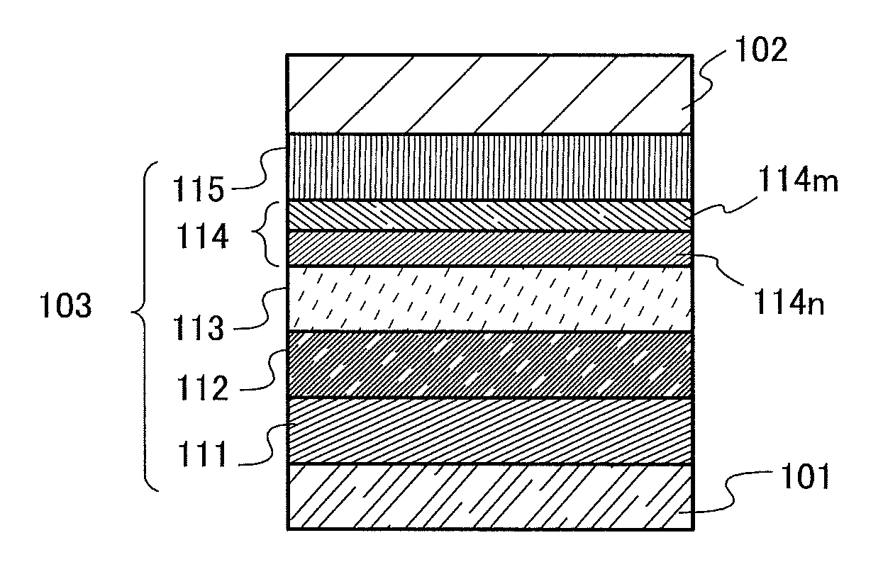
[0069]The heat resistance of a light-emitting element is known to greatly depend on the heat resistance of a material used (e.g., Tg or thermal decomposition temperature), but other factors have not been examined so much. The present inventors found out that a stacked-layer structure of a light-emitting element also affects heat resistance, and invented a light-emitting element with improved heat resistance compared with those of conventional ones, in which a layer containing NBPhen and a layer containing a condensed aromatic compound or a condensed heteroaromatic compound are stacked as an electron-transport layer.

[0070]FIG. 1A illustrates a schematic diagram of a light-emitting element of one embodiment of the present invention. The light-emitting element has at least a pair of electrodes (a first electrode 101 and a second electrode 102) and an EL layer 103 including a layer 114n containing a condensed aromatic compound or a condensed heteroaromatic compound and a layer 114m cont...

embodiment 2

[0078]In this embodiment, a detailed example of the structure of the light-emitting element described in Embodiment 1 will be described below with reference to FIG. 1A.

[0079]The light-emitting element in this embodiment includes, between the pair of electrodes, the EL layer including a plurality of layers. In this embodiment, the light-emitting element includes the first electrode 101, the second electrode 102, and the EL layer 103 which is provided between the first electrode 101 and the second electrode 102. Note that the following description is made on the assumption that the first electrode 101 functions as an anode and that the second electrode 102 functions as a cathode.

[0080]Since the first electrode 101 functions as the anode, the first electrode 101 is preferably formed using any of metals, alloys, electrically conductive compounds with a high work function (specifically, a work function of 4.0 eV or more), mixtures thereof, and the like. Specifically, for example, indium ...

embodiment 3

[0136]In this embodiment, a different embodiment of the present invention is described. In the light-emitting element described in Embodiment 1 or 2, NBPhen is used for a layer on the cathode side (the layer 114m containing NBPhen) in the electron-transport layer 114.

[0137]It is preferable that the concentration of impurities in NBPhen, particularly the concentration of NBPhen derivatives mono-substituted by chlorine, be low, in which case a highly reliable light-emitting element can be provided.

[0138]The impurity concentration of a material used for the EL layer 103 normally has an insignificant influence on a layer positioned apart from the light-emitting layer 113. However, the concentration of impurities in NBPhen solid (particularly the concentration of NBPhen derivatives mono-substituted by chlorine) has an influence on the reliability of a light-emitting element even when NBPhen exists apart from the light-emitting layer 113. Therefore, in a light-emitting element including N...


PUM


Abstract

A light-emitting element with improved heat resistance is provided without losing its advantages such as thinness, lightness, and low power consumption. A light-emitting element is provided which includes a first electrode, a second electrode, and an EL layer between the first electrode and the second electrode, in which the EL layer includes a layer containing a condensed aromatic compound or a condensed heteroaromatic compound, and a layer containing 2,9-bis(naphthalen-2-yl)-4,7-diphenyl-1,10-phenanthroline (abbreviation: NBPhen) in contact with the layer containing the condensed aromatic compound or the condensed heteroaromatic compound.

Description

BACKGROUND OF THE INVENTION[0001]1. Field of the Invention[0002]The present invention relates to an object, a method, or a manufacturing method. In addition, the present invention relates to a process, a machine, manufacture, and a composition of matter. One embodiment of the present invention particularly relates to a semiconductor device, a display device, a light-emitting device, a driving method thereof, and a manufacturing method thereof. One embodiment of the present invention particularly relates to a light-emitting element, a display module, a lighting module, a display device, a light-emitting device, an electronic device, and a lighting device in which an organic compound is used as a light-emitting substance.[0003]2. Description of the Related Art[0004]In recent years, research and development of a light-emitting element (organic EL element) which uses an organic compound and utilizes electroluminescence (EL) have been actively promoted. In the basic structure of such a l...

Claims


Application Information

Patent Timeline
IPC IPC(8): H01L51/52H01L51/00H01L51/50
CPCH01L51/529H01L51/5016H01L51/0074H01L51/006H01L51/0085H01L51/0072H01L51/0058H01L51/0054H01L51/0073H01L51/0052H10K59/17H10K59/12H10K85/622H10K85/626H10K85/636H10K85/633H10K85/615H10K85/631H10K85/6576H10K85/6574H10K85/6572H10K85/342H10K50/11H10K2101/10H10K50/166H10K2101/90C09K11/06C09K2211/1044H10K50/87
Inventor SUZUKI, TSUNENORISASAKI, TOSHIKIKATAISHI, RIHOSEO, SATOSHI
Owner SEMICON ENERGY LAB CO LTD
Why Eureka
Try Eureka