Light-emitting device and method of manufacturing the same

a technology of light-emitting devices and manufacturing methods, which is applied in the direction of lasers, semiconductor amplifier structures, semiconductor lasers, etc., can solve the problems that the semiconductor optical amplifiers for the 405-nm band have rarely been used in the practical use, and achieve the effects of high quality, no adverse effects such as deterioration of condensing characteristics, and high reliability

Active Publication Date: 2015-02-12
SONY CORP
View PDF3 Cites 4 Cited by
  • Summary
  • Abstract
  • Description
  • Claims
  • Application Information

AI Technical Summary

Benefits of technology

[0034]Therefore, the mode of a light beam to be emitted is allowed to be a single mode. Further, since a width of a slab waveguide and a thickness of the first light guide layer are substantially equal to each other, the light beam is allowed to have a sectional shape close to a perfect circle, and adverse effects such as deterioration in condensing characteristics are not caused in applications using a lens or an optical fiber.
[0035]Further, in the first method of manufacturing the light-emitting devic

Problems solved by technology

Since optical amplifiers have been developed mainly for optical communication, semic

Method used


Image

  • Light-emitting device and method of manufacturing the same
  • Light-emitting device and method of manufacturing the same
  • Light-emitting device and method of manufacturing the same

Examples


example 4 (modification of any of examples 1 to 3)

5. Example 4 (Modification of any of Examples 1 to 3)

[0051]6. Example 5 (Modification of any of Examples 1 to 4), and others

[0052]In a third method of manufacturing a light-emitting device according to the present disclosure, for example, a growth inhibition layer may be preferably configured of a material layer of one or more kinds selected from a group configured of SiO2, Al2O3, MN, ZrO2, Ta2O5, and AlGaInN.

[0053]In a light-emitting device in any of first to third methods of manufacturing a light-emitting device according to the present disclosure or a light-emitting device according to the present disclosure that has the above-described preferred mode, it may be desirable to satisfy t1≦3×10⁻⁶ m. When crystal growth is performed to allow a thickness t1 of a first guide layer to be equal to or smaller than 3×10⁻⁶ m, crystal growth surface morphology is not roughened, and deterioration in light emission characteristics and electrical characteristics of the light-emitting device is p...

example 1

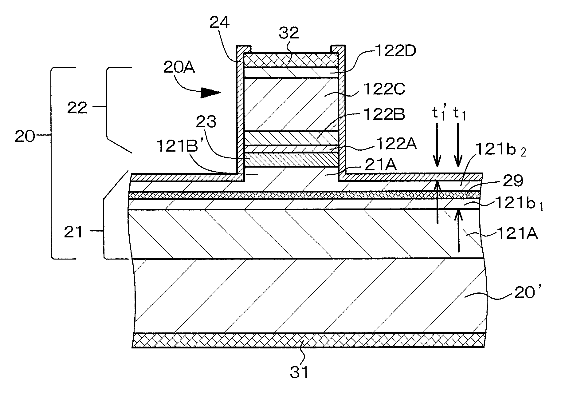
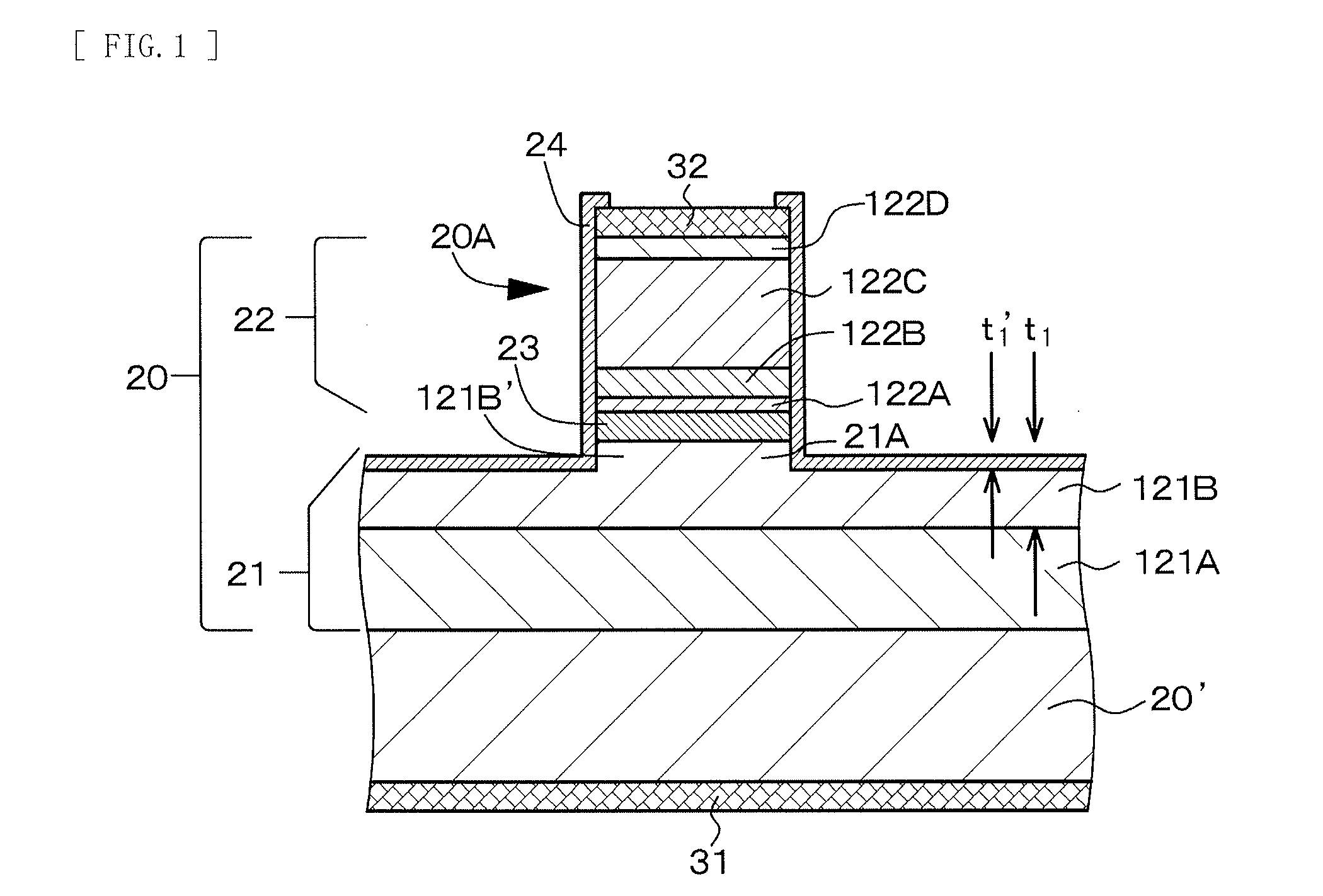
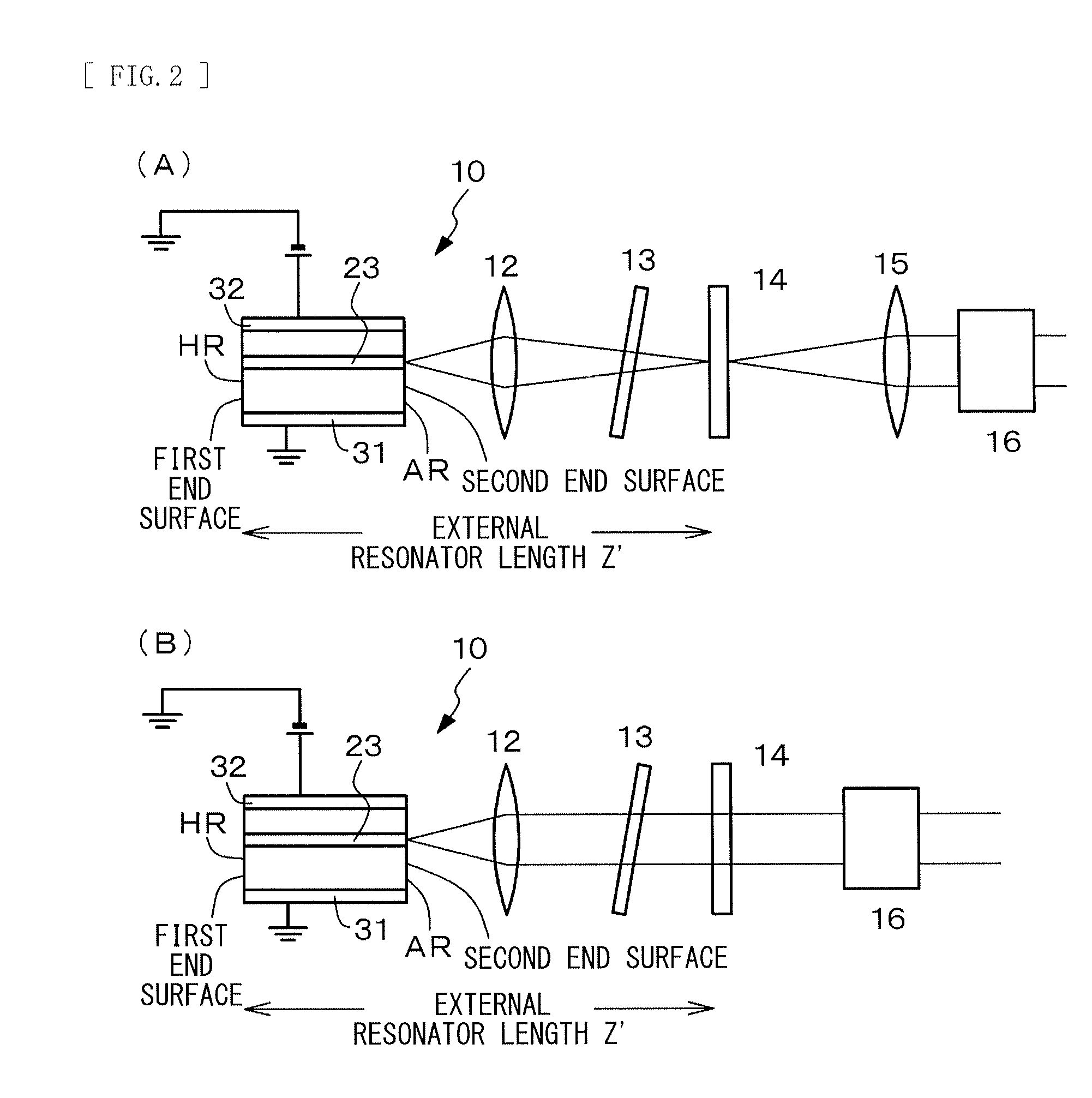
[0077]Example 1 relates to the light-emitting device according to the present disclosure, and the first method of manufacturing the light-emitting device according to the present disclosure. Specifically, a light-emitting device of Example 1 is a laser diode device, and as illustrated in a schematic partial sectional view taken along a virtual plane perpendicular to an axis line of the light-emitting device in FIG. 1, the light-emitting device of Example 1 includes a laminate structure body 20 configured by laminating, in order, a first compound semiconductor layer 21 of a first conductivity type, an active layer (a light emission region or a gain region) 23 made of a compound semiconductor, and a second compound semiconductor layer 22 of a second conductivity type different from the first conductivity type on a base substrate 20′, a second electrode 32 formed on the second compound semiconductor layer 22, and a first electrode 31 configured to be electrically connected to the first...

example 2

[0104]Example 2 is a modification of the light-emitting device of Example 1, and relates to the second method of manufacturing the light-emitting device according to the present disclosure. Specifically, a light-emitting device of Example 2 is also a laser diode device, and as illustrated in a schematic partial sectional view taken along a virtual plane perpendicular to an axis line of the light-emitting device in FIG. 7(C), two recess sections 25 extending along an axis line direction of the light-emitting device are formed in the base substrate 20′. Then, the laminate structure body 20 described in Example 1 is formed entirely, i.e., on the two recess sections 25 and a region 26 sandwiched between the two recess sections 25 of the base substrate 20′. Moreover, the second electrode 32 is disposed above the region 26 of the base substrate 20′.

[0105]In this case, the first compound semiconductor layer 21 has a laminate structure including a first cladding layer and a first light guid...


PUM


Abstract

Provided is a high-output light-emitting device capable of emitting a light beam in a single mode. The light-emitting device includes a laminate structure body configured by laminating, in order, a first compound semiconductor layer, an active layer, and a second compound semiconductor layer on a base substrate, a second electrode, and a first electrode. The first compound semiconductor layer has a laminate structure including a first cladding layer and a first light guide layer in order from the base substrate, and the laminate structure body has a ridge stripe structure configured of the second compound semiconductor layer, the active layer, and a portion in a thickness direction of the first light guide layer. Provided that a thickness of the first light guide layer is t1, and a thickness of the portion configuring the ridge stripe structure of the first light guide layer is t1′, 6×10⁻⁷ m<t1 and 0(m)<t1′≦0.5·t1 are satisfied.

Description

TECHNICAL FIELD[0001]The present disclosure relates to a light-emitting device and a method of manufacturing the same.BACKGROUND ART[0002]In laser light sources, power enhancement is a major task. Therefore, in addition to output enhancement in laser diode devices, semiconductor optical amplifiers (SOA) have been diligently studied as devices that amplify light from a laser light source. As used herein, optical amplifiers refer to amplifiers that directly amplify an optical signal in the form of light without converting the optical signal into an electrical signal, and the optical amplifiers have a laser structure without resonator, and amplify incident light with an optical gain thereof.[0003]Since optical amplifiers have been developed mainly for optical communication, semiconductor optical amplifiers for a 405-nm band have rarely been put to practical use. A semiconductor optical amplifier for a 1.5-μm band that uses a GaInAsP-based compound semiconductor and has a tapered ridge ...

Claims


Application Information

Patent Timeline
IPC IPC(8): H01S5/22H01S5/32H01S5/20H01S5/50H01S5/343
CPCH01S5/22H01S5/50H01S5/3213H01S5/2031H01S5/34333B82Y20/00H01S5/141H01S5/2009H01S5/209H01S5/305H01S5/3063H01S5/309H01S5/3211H01S2301/166H01S2301/176
Inventor KURAMOTO, MASARUKODA, RINTAROWATANABE, HIDEKI
Owner SONY CORP
Why Eureka
Try Eureka