Scanning ion microscope and secondary particle control method

a scanning ion microscope and secondary particle technology, applied in the field of scanning ion microscopes, can solve the problems of specimen image distortion with respect to actual image, inability to completely solve the problem of reducing the electrification of the specimen, and the existence of electric charge or secondary electron in the transmitted beam has not been paid attention, so as to prevent the distortion of the observation image

Active Publication Date: 2015-02-19
HITACHI HIGH-TECH CORP
View PDF4 Cites 2 Cited by
  • Summary
  • Abstract
  • Description
  • Claims
  • Application Information

AI Technical Summary

Benefits of technology

[0025]According to the present invention, it is possible to observe a specimen minutely and prevent distortion of an observation image even if a specimen containing insulators is charged partially.

Problems solved by technology

In a case where a specimen containing an insulator is observed with a scanning ion microscope, there is an issue that an image of the specimen is distorted with respect to an actual image as a result of the path of the ion beam being locally bent by partial electrification of the specimen.
This cannot be completely solved by reducing electrification on the specimen.
Furthermore, since the conventional thin film utilizing method described in Patent Document 9 does not care about convergence characteristics of the beam, existence of electric charge or secondary electrons in the transmitted beam has not been paid attention.

Method used


Image

  • Scanning ion microscope and secondary particle control method
  • Scanning ion microscope and secondary particle control method
  • Scanning ion microscope and secondary particle control method

Examples


first embodiment

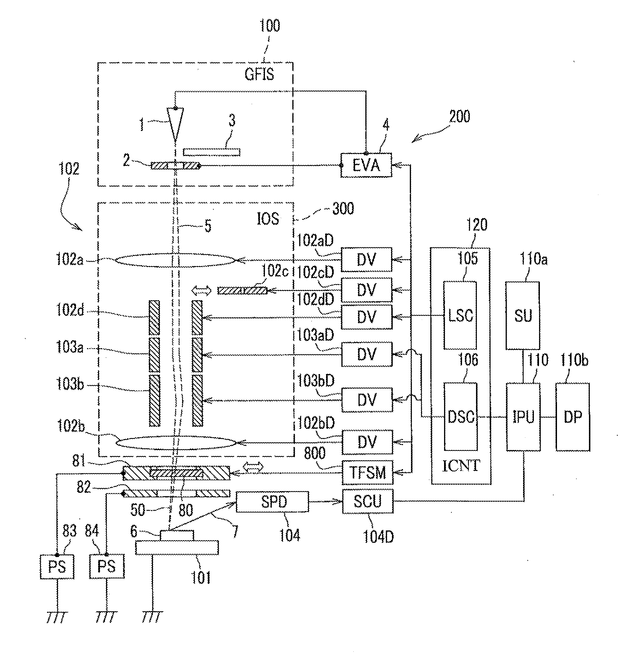
[0036]FIG. 1 shows an entire configuration of a scanning ion microscope according to the present embodiment. The scanning ion microscope 200 according to the present embodiment is configured by incorporating a gas field ionization ion source (GFIS) 100 utilizing helium (He) into a focused ion beam (FIB) device produced for a conventional gallium-liquid metal ion source (Ga-LMIS) instead of the Ga-LMIS.

[0037]In FIG. 1, a scanning ion microscope 200 has a configuration in which a helium (He) ion beam 5 emitted from a GFIS 100 enter into an ion optical system 300 (ion optical series system) which cause the ion beams 5 to converge by the ion optical system 300, and thus irradiates a specimen 6 placed on a specimen stage 101 with the ion beams 5. Acceleration voltage of ions is 30 kV.

[0038]The GFIS 100 includes: an emitter tip 1; an extraction electrode 2; and a gas discharge outlet 3 of gas supplying piping, which supplies gas for ionization to an apex of the emitter tip. The emitter ti...

second embodiment

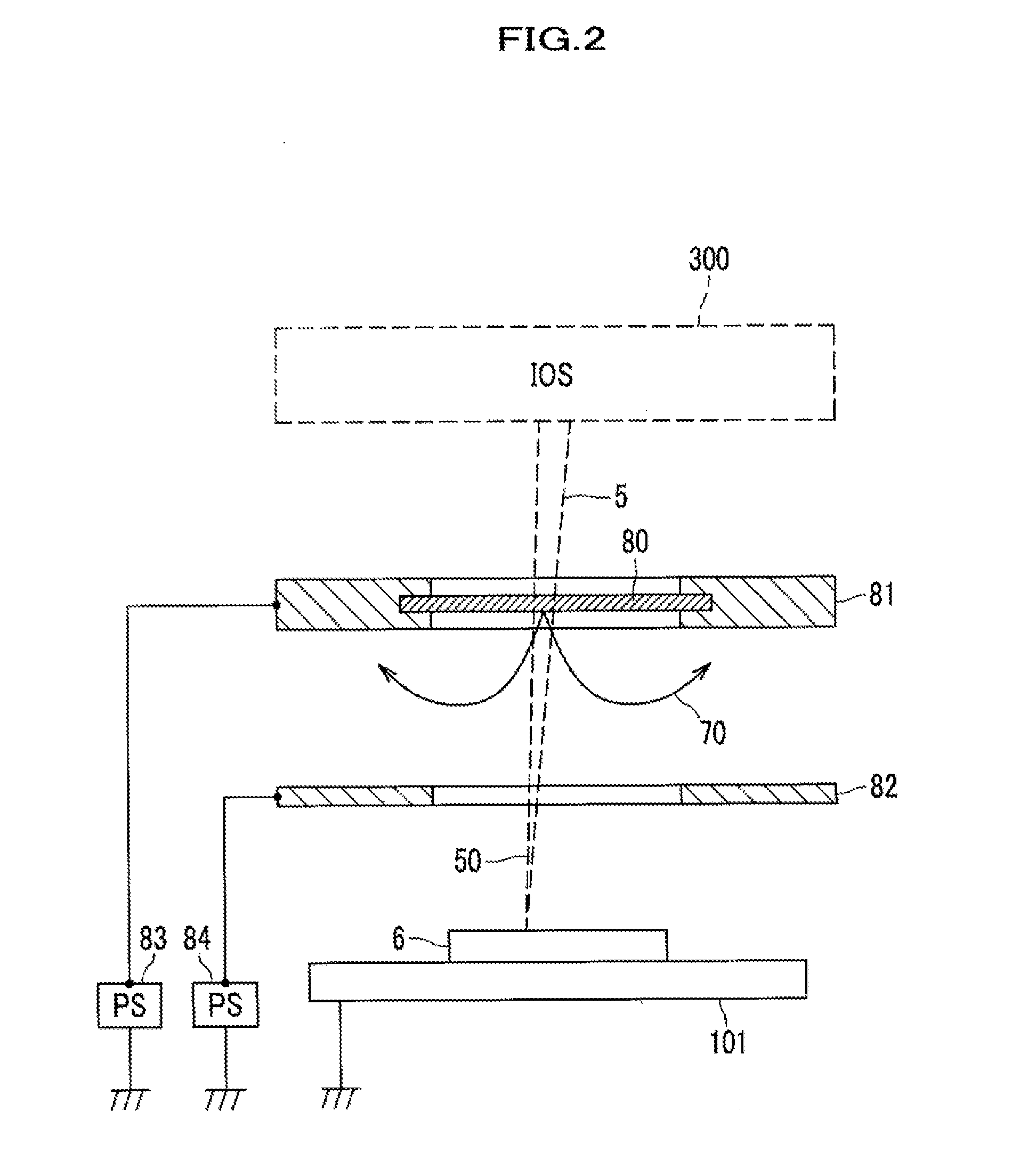
[0067]FIG. 3 shows a configuration near a thin film of the scanning ion microscope according to a second embodiment of the present invention. The scanning ion microscope in the present embodiment is fundamentally the same as that in FIG. 1 but is different in that there are additional elements near the thin film 80. FIG. 3 shows a peripheral portion of the thin film80.

[0068]If the thin film 80 is irradiated with the ion beam 5, a small amount of reflection particles and secondary electrons 71 are emitted to the side of the ion optical system 300. When they enter an electrostatic lens or a deflector in the ion optical system 300, the operation of the ion optical system 300 may become unstable as a result of inducement of unnecessary electrification onto the insulator portion. Accordingly, in the present embodiment, a shielding body 85 having an opening is arranged above the thin film 80 for blocking the reflection particles and secondary electrons 71. Although a part of the particles...

third embodiment

[0070]FIG. 4 shows a configuration near a thin film of the scanning ion microscope according to a third embodiment of the present invention. The scanning ion microscope in the present embodiment is fundamentally the same as that shown in FIG. 1 but is different in that there are additional elements near the thin film 80. FIG. 4 shows a peripheral portion of the thin film 80. It has a feature of having a several-molecules layer of ionic liquid 80a dispersed on the silicon nitride thin film 80 similar to the first embodiment. Here, C10H15F6N3O4S2 (C10H15F6N3O4S2) (CAS No. 174899-83-3) is used for the ionic liquid 80a.

[0071]In the present embodiment, since the thin film 80 effectively becomes electrically-conductive as a result of the ionic liquid 80a, restrictions in selecting the material for the thin film 80 itself are freed. That is, the thin film 80 may be a complete insulator. Since the acceleration voltage of the ion beam 5 is low, it is effective even when the electrical condu...


PUM


Abstract

The present invention is provided to enable a detailed inspection of a specimen and preventing a distortion of an observation image even when a specimen containing an insulating material is partially charged. For a scanning ion microscope utilizing a gas field ionization ion source, a thin film is disposed between an ion optical system and a specimen, and an ion beam is applied to and transmitted through this thin film in order to focus a neutralized beam on the specimen. Furthermore, an electrode for regulating secondary electrons discharged from this thin film is provided in order to eliminate mixing of noises into an observation image.

Description

FIELD OF THE INVENTION[0001]The present invention relates to a scanning ion microscope that can form a specimen image by scanning with uncharged particles and a secondary particle control method.BACKGROUND ART[0002]Patent Document 1 and Patent Document 2 disclose focused ion beam (FIB) devices that have gas field ionization ion source (GFIS) and use gas ions such as hydrogen (H2), helium (He), and neon (Ne). Such gas focused ion beams (gas FIB) has an advantageous effect in that they do not bring Ga contamination to the specimen as in a gallium (Ga: metal) focused ion beam (Ga-FIB) from a liquid metal ion source (LMIS), which is used often nowadays.[0003]In addition, the energy width of the gas ions extracted from GFIS is narrow and the size of an ion generation source is small in GFIS, and thus GFIS can form minute beams than Ga-FIB.[0004]Such gas FIB devices are used as a scanning ion microscope having a high resolution. That is, an image of the specimen is formed by detecting sec...

Claims


Application Information

Patent Timeline
Patent Type & Authority Applications(United States)
IPC IPC(8): H01J37/28H01J37/20H01J37/22H01J37/26H01J37/244
CPCH01J37/28H01J37/265H01J37/244H01J37/222H01J2237/0807H01J2237/2806H01J2237/2807H01J2237/0473H01J37/20H01J37/317
Inventor KAWANAMI, YOSHIMIOSE, YOICHI
Owner HITACHI HIGH-TECH CORP
Why Eureka
Try Eureka