
Titanium incorporation into absorber layer for solar cell

a solar cell and absorber layer technology, applied in the direction of sustainable manufacturing/processing, climate sustainability, semiconductor devices, etc., can solve the problems of large vsub>oc/sub>deficit of czts devices, difficult to achieve an efficiency above 11%, and relatively low performance of czts solar cells

Inactive Publication Date: 2015-03-05
GLOBALFOUNDRIES INC
View PDF10 Cites 6 Cited by
  • Summary
  • Abstract
  • Description
  • Claims
  • Application Information

AI Technical Summary

Benefits of technology

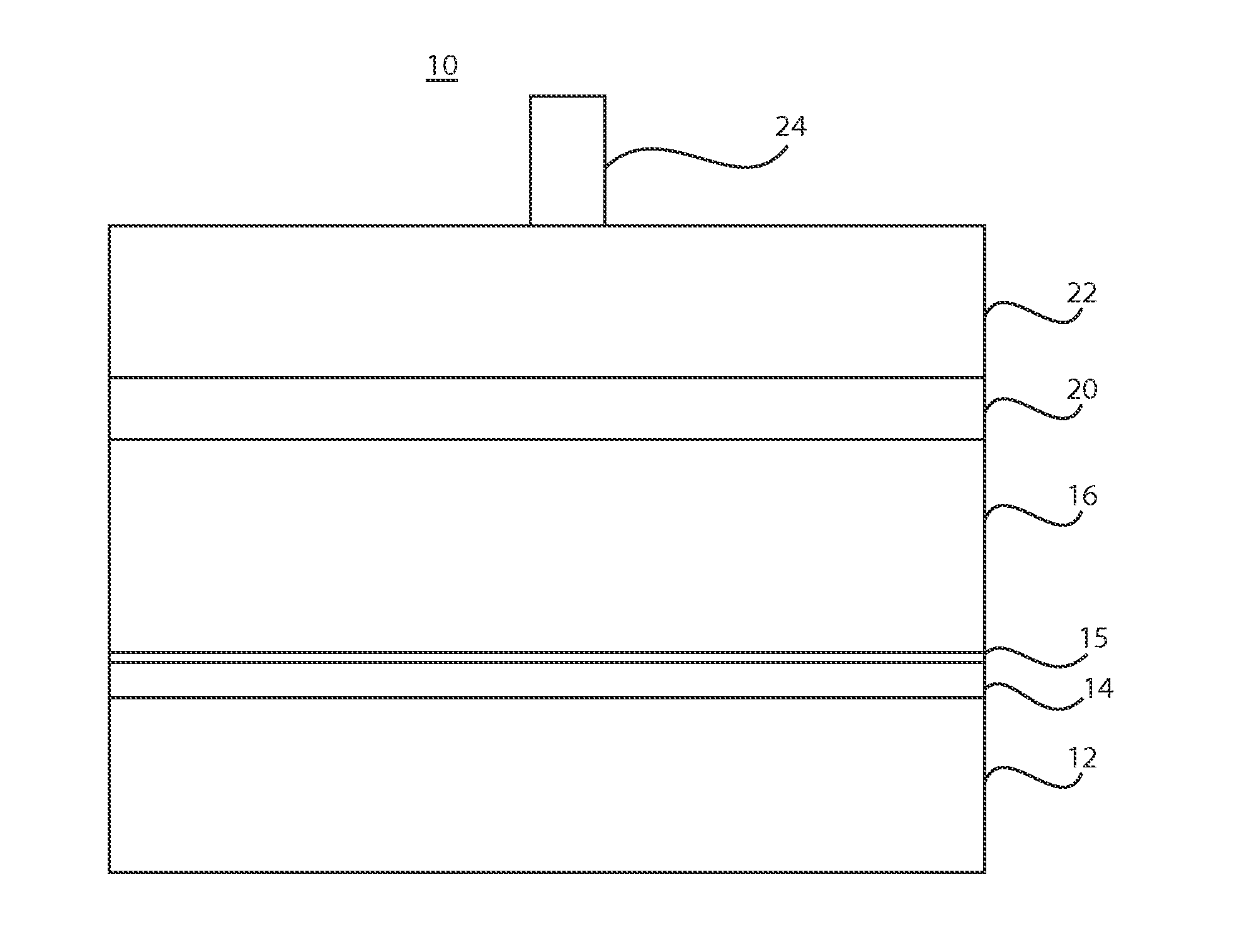
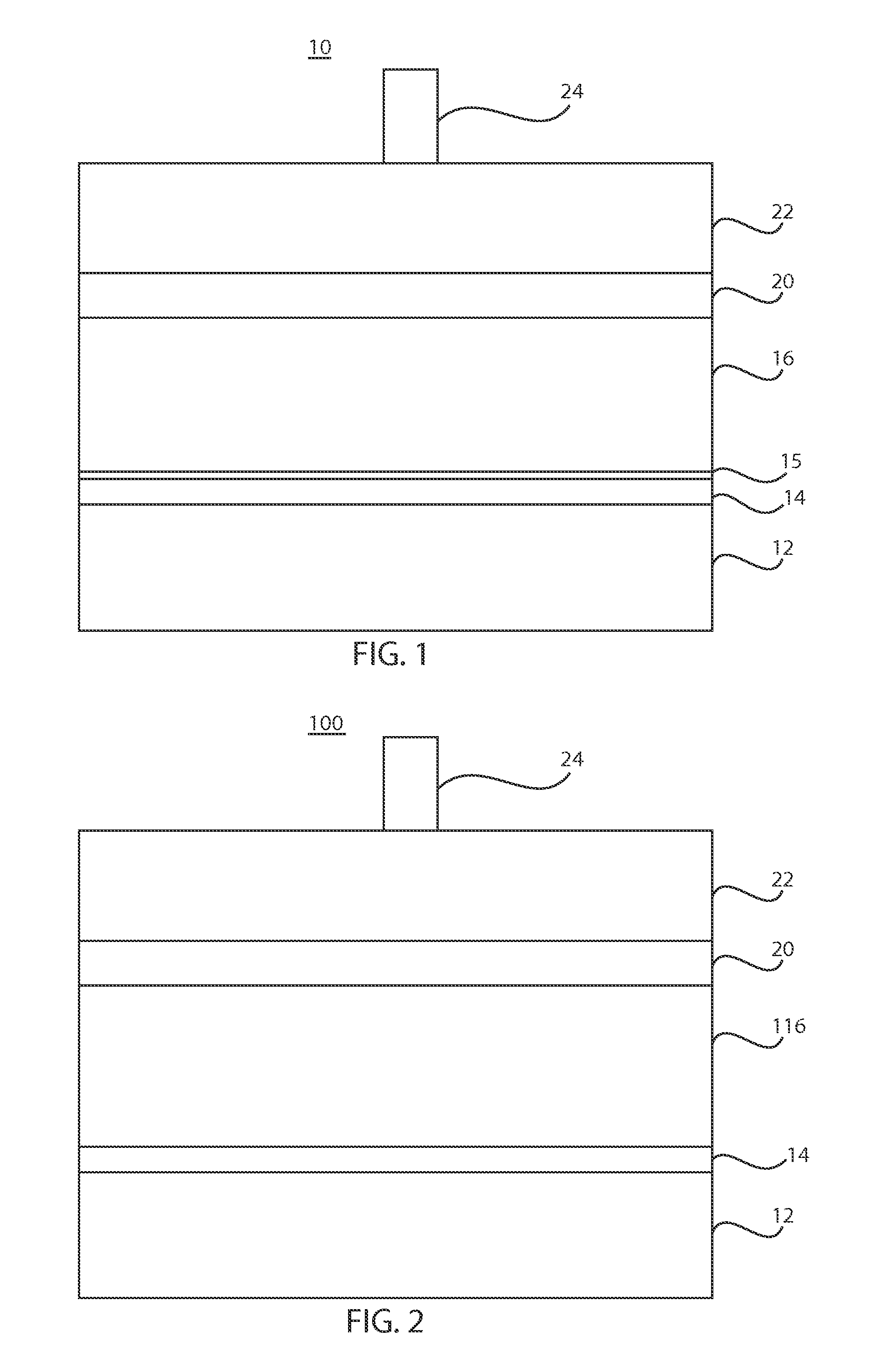
This patent describes methods for fabricating a photovoltaic device by depositing layers of titanium and a chalcogenide compound on a conductive layer on a substrate, then annealing them to recrystallize the chalcogenide material. Another method involves depositing a layer of titanium doped with copper, zinc, and stannum on a conductive layer, then annealing to recrystallize the chalcogenide material. The resulting device has improved efficiency and performance compared to conventional photovoltaic devices.

Problems solved by technology

However, it is very difficult to achieve an efficiency above 11%, and the PCE of CZTS solar cells is still far below the physical limit, known as the Shockley-Queisser (SQ) limit, of about 29% under terrestrial conditions.
One fundamental reason for the relatively low performance of CZTS solar cells is the large Voc deficit of CZTS devices.
Thus far, no effective method exists that solves the high Voc deficit issue.

Method used


Image

  • Titanium incorporation into absorber layer for solar cell
  • Titanium incorporation into absorber layer for solar cell
  • Titanium incorporation into absorber layer for solar cell

Examples


example 1

[0057]For making Ti-free devices, solution A (3.3M Cu2S) was made by dissolving Cu and S in hydrazine. Similarly, Sn and Se were stirred in hydrazine to form slurry B (1.5 M SnSes); Solution A and slurry B were mixed together and transferred to a vial containing zinc formate, yielding solution C with final composition Cu / (Zn+Sn)=0.8, Zn / Sn=1.22 and nominal kesterite CZTSSe concentration of approximately 0.4 M. The thin film CZTS absorber layer with final thickness of 2-2.5 microns was prepared by spin coating this mixture over six consecutive layers at 600 rpm and then subsequently subjecting it to a short anneal on a ceramic hot plate with a set point of 630 degrees C.

[0058]The CdS buffer, ZnO window, and indium doped tin oxide (ITO) layers were subsequently deposited by chemical bath deposition and RF magnetron sputtering, respectively, giving a CZTSSe device structure with a device area of approximately 0.45 cm2, as defined by mechanical scribing. A Ni / Al collection grid and 110-...

example 2

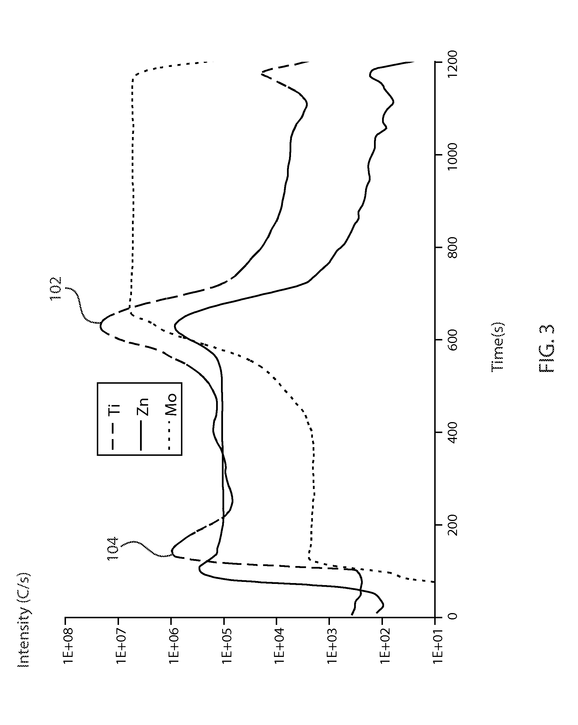
[0059]For making Ti-incorporating devices, a solution A (3.3M Cu2S) was made by dissolving Cu and S in hydrazine. Similarly, Sn and Se were stirred in hydrazine to form slurry B (1.5 M SnSes); Solution A and slurry B were mixed together and transferred to a vial containing zinc formate, yielding solution C with final composition Cu / (Zn+Sn)=0.8, Zn / Sn=1.22 and nominal kesterite CZTSSe concentration of approximately 0.4 M. A 20 nm titanium thin film was deposited on molybdenum-coated glass by electron-beam evaporation. The Ti- and Mo-coated glass was used as a substrate for CZTS deposition.

[0060]The thin film CZTS absorber layer with final thickness of 2-2.5 microns was prepared by spin coating this mixture over six consecutive layers at 600 rpm and then subsequently subjecting it to a short anneal on a ceramic hot plate with a set point of 630 degrees C. The CdS buffer, ZnO window, and indium doped tin oxide (ITO) layers were subsequently deposited by chemical bath deposition and RF ...


PUM

PropertyMeasurementUnit
thicknessaaaaaaaaaa
thicknessaaaaaaaaaa
open circuit voltageaaaaaaaaaa

Abstract

A method for fabricating a photovoltaic device includes forming a film including titanium on a conductive layer formed on a substrate. An absorber layer is formed including a Cu—Zn—Sn containing chalcogenide compound with a kesterite structure of the formula: Cu2-xZn1+ySn(S1-zSez)4+q wherein 0≦x≦1; 0≦y≦1; 0≦z≦1; −1≦q≦1 (CZTS) on the film. The absorber layer is annealed to diffuse titanium therein and to recrystallize the CZTS material of the film. A buffer layer is formed on the absorber layer, and a transparent conductive layer is formed on the buffer layer.

Description

RELATED APPLICATION DATA[0001]This application is a Continuation application of co-pending U.S. patent application Ser. No. 14 / 013,827 filed on Aug. 29, 2013, incorporated herein by reference in its entirety.BACKGROUND[0002]1. Technical Field[0003]The present invention relates to photovoltaic devices and fabrication methods, and more particularly to earth-abundant photovoltaic material having a titanium doped absorber layer.[0004]2. Description of the Related Art[0005]Cu2ZnSnSxSe4-x (CZTS) is a promising earth-abundant photovoltaic material for high-efficiency thin film solar cells. A power conversion efficiency (PCE) of 11.1% has been achieved by Teodor K. Todorov, et al. using a hydrazine-assisted solution approach (Adv. Energy Mater. 3, 34-38, 2013). Other vacuum-based and non-vacuum-based deposition techniques have also been successfully utilized to fabricate CZTS solar cells with PCE above 9%. However, it is very difficult to achieve an efficiency above 11%, and the PCE of CZTS...

Claims


Application Information

Patent Timeline
Patent Type & Authority Applications(United States)
IPC IPC(8): H01L31/032
CPCH01L31/0327H01L31/0326H01L31/1864H01L31/1872Y02E10/50Y02P70/50
Inventor HOPSTAKEN, MARINUS J.MITZI, DAVID B.WANG, WEIWINKLER, MARK T.
Owner GLOBALFOUNDRIES INC
Learn More