Imaging device
a technology of a flat panel detector and an imager, which is applied in the direction of x/gamma/cosmic radiation measurement, radioation controlled devices, instruments, etc., can solve the problems increasing power consumption, and achieves the effect of reducing the reliability of a flat panel detector, increasing power consumption, and high stability
- Summary
- Abstract
- Description
- Claims
- Application Information
AI Technical Summary
Benefits of technology
Problems solved by technology
Method used
Image
Examples
embodiment 1
[0057]In this embodiment, an imaging device using radiation such as X-rays, which is one embodiment of the present invention, will be described with reference to drawings.
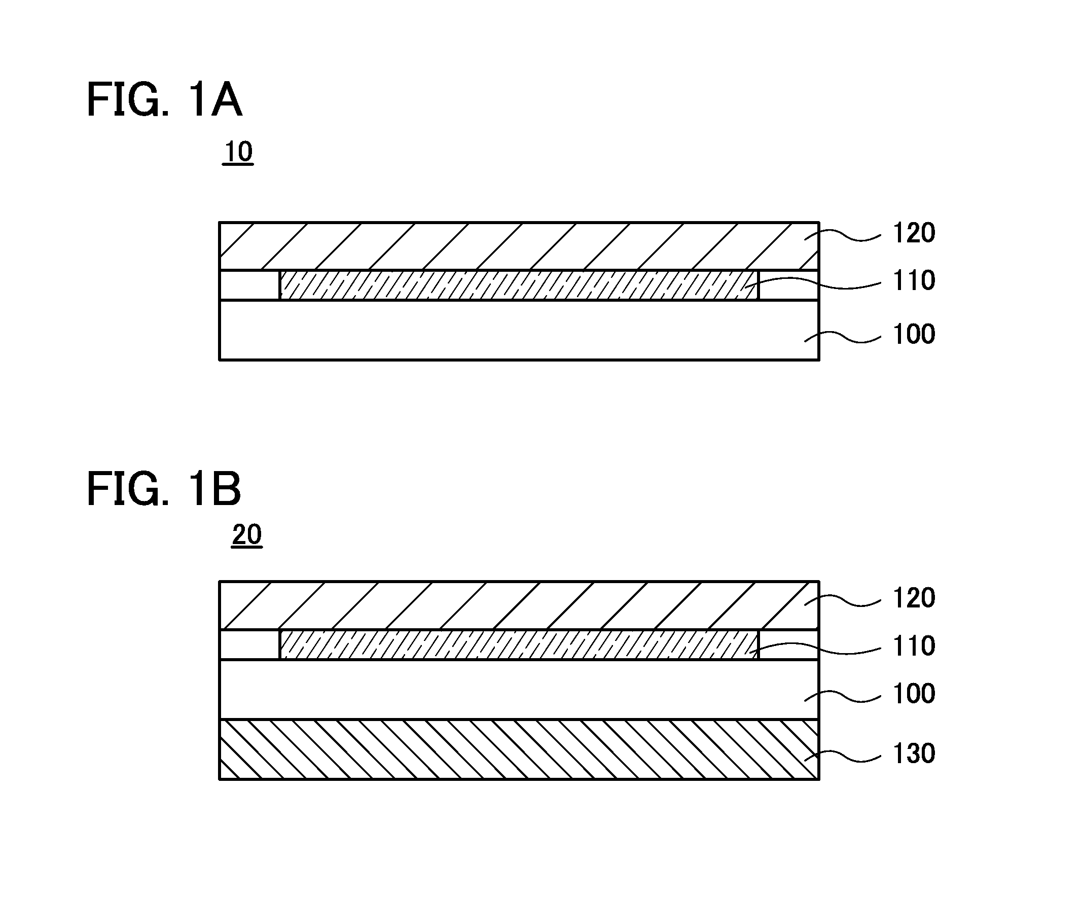
[0058]FIGS. 1A and 1B are cross-sectional views each illustrating a structure of the imaging device of one embodiment of the present invention. An imaging device 10 illustrated in FIG. 1A includes a pixel array 110 over a substrate 100, and a scintillator 120 over the pixel array 110.
[0059]The scintillator 120 is made of a substance that, when exposed to radiation such as X-rays or gamma-rays, absorbs the energy of the rays to emit visible light or ultraviolet light or a material containing the substance. Examples of the known materials include Gd2O2S:Tb, Gd2O2S:Pr, Gd2O2S:Eu, BaFCl:Eu, NaI, CsI, CaF2, BaF2, CeF3, LiF, LiI, and ZnO, and a resin or ceramics in which any of the materials is dispersed.
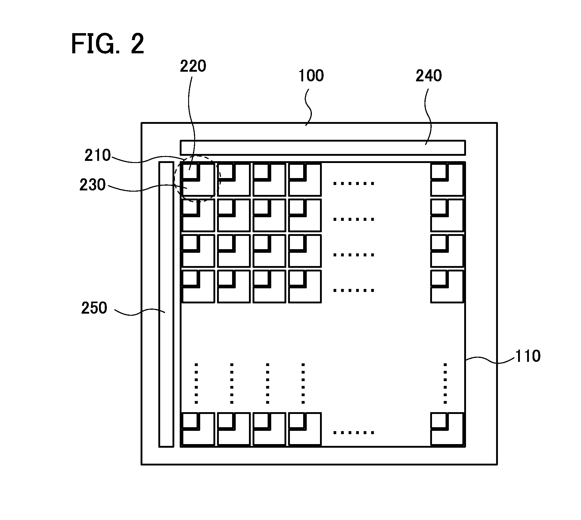
[0060]The pixel array 110 over the substrate 100 can have a structure illustrated in the top view of FIG. 2, for examp...
embodiment 2
[0085]In this embodiment, the pixel circuit 210 shown in Embodiment 1 will be described.
[0086]FIG. 7A shows an example of a circuit that can be used as the pixel circuit 210 illustrated in FIG. 2. A circuit 211 includes a photodiode 320 serving as the light-receiving element 220, and a first transistor 301, a second transistor 302, and a third transistor 303 that are provided in the circuit portion 230 connected to the light-receiving element 220.
[0087]An anode of the photodiode 320 is electrically connected to a first wiring 311 (RS); a cathode of the photodiode 320 is electrically connected to one of a source and a drain of the first transistor 301; the other of the source and the drain of the first transistor 301 is electrically connected to a wiring 305 (FD); a gate of the first transistor 301 is electrically connected to a second wiring 312 (TX); one of a source and a drain of the second transistor 302 is electrically connected to a fourth wiring 314 (GND); the other of the sou...
embodiment 3
[0133]In this embodiment, an example of the imaging device using radiation such as X-rays, which is different from that shown in Embodiment 1, will be described with reference to drawings. Note that components similar to those in Embodiment 1 are denoted by the same reference numerals and are not described in detail.
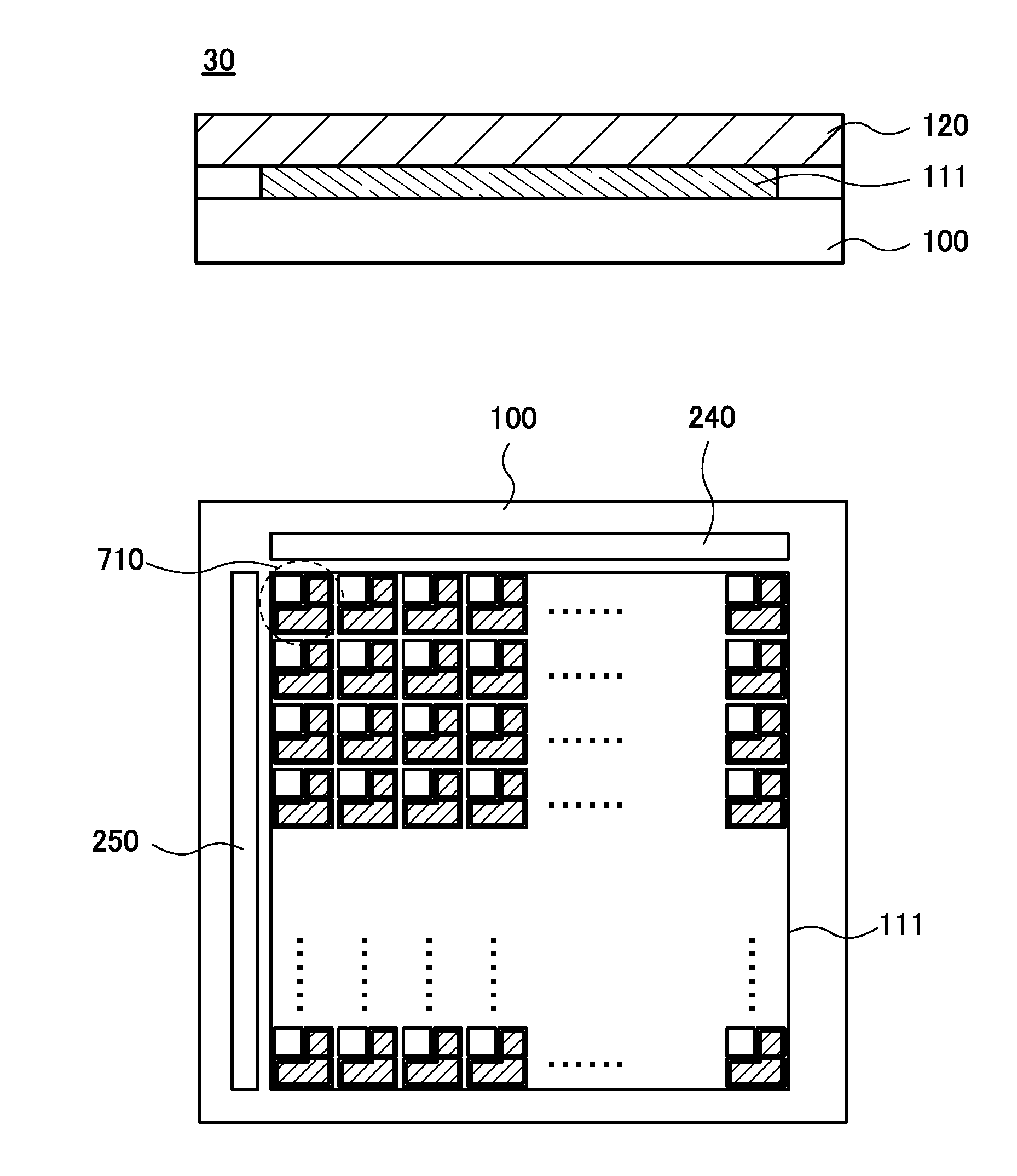
[0134]FIGS. 13A and 13B are cross-sectional views each illustrating a structure of the imaging device of one embodiment of the present invention. An imaging device 30 illustrated in FIG. 13A includes a pixel array 111 over the substrate 100, and the scintillator 120 over the pixel array 111.
[0135]The pixel array 111 over the substrate 100 can have a structure illustrated in the top view of FIG. 13B, for example. Note that in FIG. 13B, the scintillator 120 is omitted for clarity.
[0136]The pixel array 111 includes a plurality of pixel circuits 710 arranged in a matrix, and the pixel circuits 710 each include a light-receiving element 720 and an imaging circuit portion 730 ...
PUM
 Abstract
Description
Claims
Application Information


