Organic electroluminescent display device and method of manufacturing the same

Active Publication Date: 2015-03-12
JAPAN DISPLAY INC
View PDF2 Cites 62 Cited by
  • Summary
  • Abstract
  • Description
  • Claims
  • Application Information

AI Technical Summary

Benefits of technology

[0016](8) According to the present invention, there is provided an organic electroluminescent display device, including: a substrate; a plurality of pixel electrodes that are disposed on the substrate; an organic electroluminescent film that is disposed on the substrate with the inclusion of a common layer which continuously covers the plurality of pixel electrodes; and a common electrode that is disposed on the organic electroluminescent film, in which the common layer has low conductive portions lower in electric conductivity than portions above the plurality of pixel electrodes, above the areas between the respective adjacent pixel electrodes. According to the present invention, since the common layer of the organic electroluminescent film is lower in electric conductivity above the areas between the respective adjacent pixel electrodes, the current leakage between the adjacent pixel electrodes can be prevented.
[0017](9) According to the present invention, there is provided an organic electroluminescent display device, including: a substrate; a plurality of pixel electrodes that are disposed on the substrate; an insulating layer that is disposed in areas between the respective adjacent pixel electrodes so as to rest on ends of the respective pixel electrodes

Problems solved by technology

There arises such a problem that the current leakage causes the adjacent pixels to

Method used


Image

  • Organic electroluminescent display device and method of manufacturing the same
  • Organic electroluminescent display device and method of manufacturing the same
  • Organic electroluminescent display device and method of manufacturing the same

Examples


first embodiment

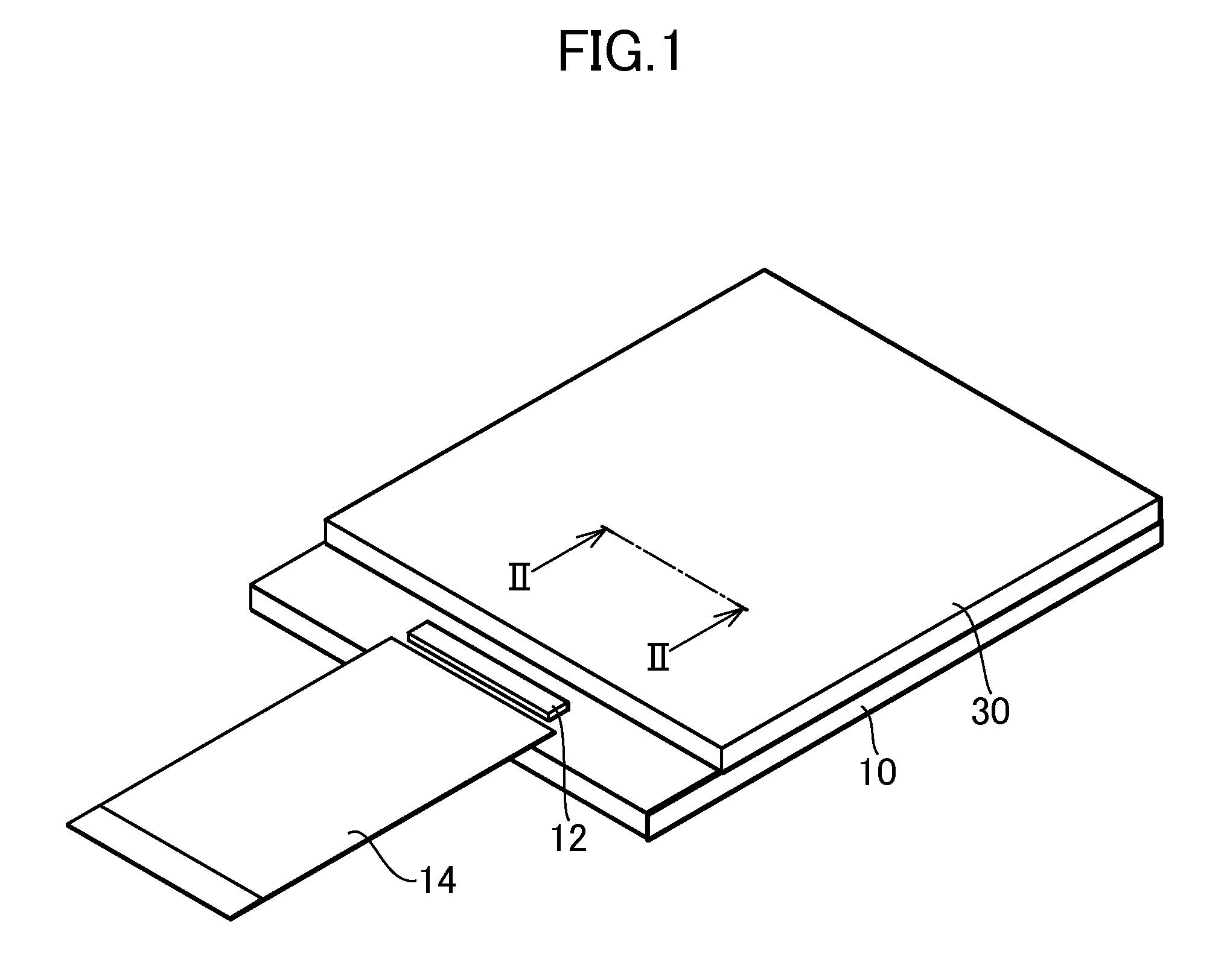
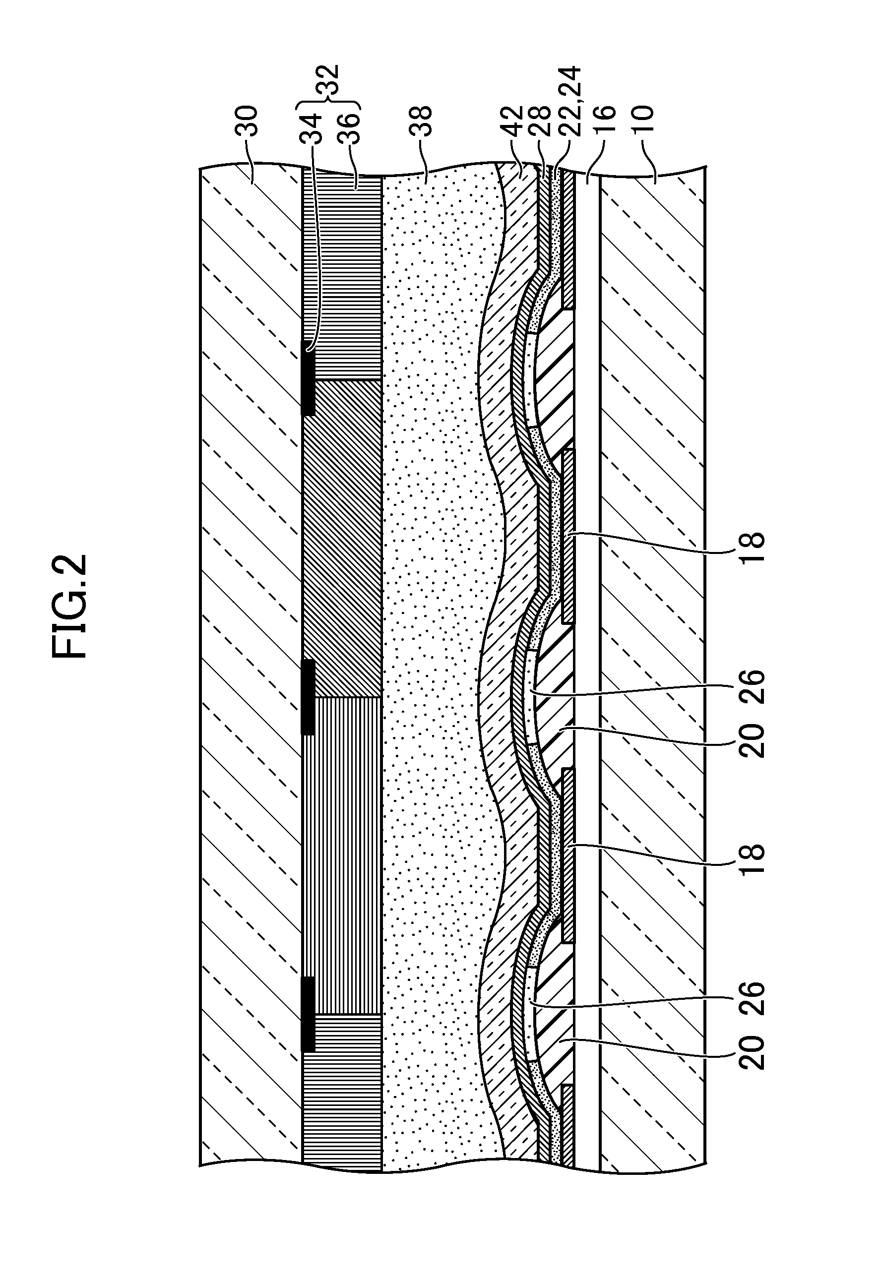
[0047]Hereinafter embodiments of the present invention will be described with reference to the accompanying drawings. FIG. 1 is a perspective view of an organic electroluminescent display device according to the present invention. FIG. 2 is a schematic cross-sectional view taken along a line II-II of the organic electroluminescent display device illustrated in FIG. 1.

[0048]As illustrated in FIG. 1, the organic electroluminescent display device includes a first substrate 10 having an optical transparency made of glass or the like. The first substrate 10 has an image display area for image display. An integrated circuit chip 12 for driving an element for displaying an image is mounted on the first substrate 10. A flexible wiring substrate 14 is connected to the first substrate 10 for electric connection with an external.

[0049]As illustrated in FIG. 2, a circuit layer 16 is disposed on the first substrate 10. The circuit layer 16 includes lines, thin film transistors, and an insulating...

second embodiment

[0067]FIG. 8 is a perspective view of an organic electroluminescent display device according to the present invention. FIG. 9 is a schematic cross-sectional view taken along a line IX-IX of the organic electroluminescent display device illustrated in FIG. 8.

[0068]As illustrated in FIG. 8, the organic electroluminescent display device includes a first substrate 110 having an optical transparency made of glass or the like. The first substrate 110 has an image display area for image display. An integrated circuit chip 112 for driving an element for displaying an image is mounted on the first substrate 110. A flexible wiring substrate 114 is connected to the first substrate 110 for electric connection with an external.

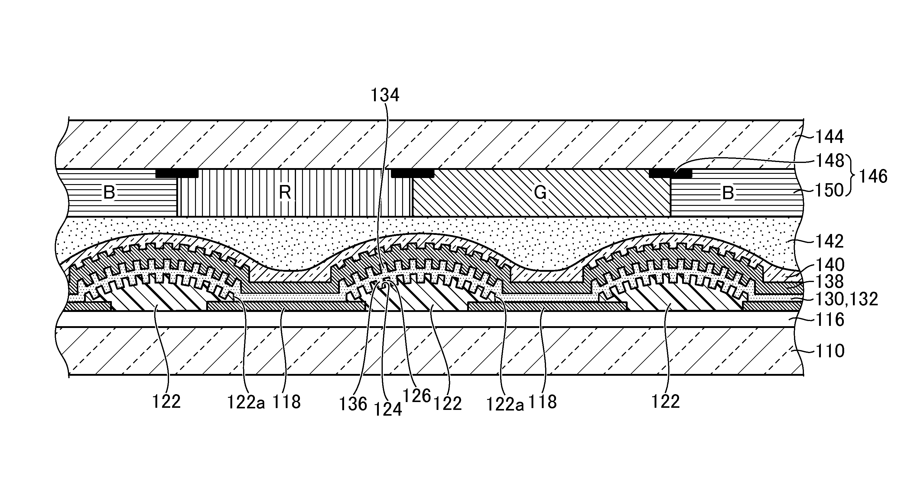
[0069]As illustrated in FIG. 9, a circuit layer 116 is disposed on the first substrate 110. The circuit layer 116 includes lines, thin film transistors, an insulating film and the like not shown. Plural pixel electrodes 118 are disposed on the first substrate 110 (on the c...

third embodiment

[0086]FIG. 15 is a cross-sectional view of an organic electroluminescent display device according to the present invention. In this embodiment, a concavo-convex shape of an insulating layer 222 is formed on a plane. That is, bottom surfaces of plural concave portions 224 are arrayed along one plane, and upper surfaces of plural convex portions 226 are arrayed along another plane. Plural sealing films 240 (a first sealing film 256, a second sealing film 258, and a third sealing film 260) are disposed on a common electrode 238. The sealing films 240 seal an organic electroluminescent film 230 to block moisture. The other configurations correspond to the contents described in the above embodiments.

[0087]FIGS. 16 and 17 are diagrams illustrating a method of manufacturing the organic electroluminescent display device according to the third embodiment of the present invention.

[0088]As illustrated in FIG. 16, a concavo-convex shape is given an insulating material 252 formed to cover plural...


PUM


Abstract

A substrate on which a plurality of pixel electrodes are disposed is prepared. An organic electroluminescent film 22 is formed with the inclusion of a common layer that continuously covers the plural pixel electrodes. A common electrode is formed on the organic electroluminescent film. The common layer is irradiated with an energy ray above areas between the respective adjacent pixel electrodes with the avoidance of irradiation above the plural pixel electrodes. An electric conductivity of the common layer is reduced above the areas between the respective adjacent pixel electrodes, by irradiation of the energy ray. With this configuration, a current leakage can be prevented between the adjacent pixels.

Description

CROSS-REFERENCE TO RELATED APPLICATION[0001]The present application claims priorities from Japanese application JP2013-186146 filed on Sep. 9, 2013, and Japanese application JP2013-186175 filed on Sep. 9, 2013, the contents of which are hereby incorporated by reference into this application.BACKGROUND OF THE INVENTION[0002]1. Field of the Invention[0003]The present invention relates to an organic electroluminescent display device and a method of manufacturing the display device.[0004]2. Description of the Related Art[0005]An organic electroluminescent display device has a structure in which an organic film is sandwiched between an anode and a cathode. Normally, plural organic films are laminated on each other, and include a light emitting layer as one layer. In order to obtain light emission of one color (for example, white) in plural pixels, the organic film forming the light emitting layer is wholly continuously disposed. Alternatively, in order to obtain light emission of plural ...

Claims


Application Information

Patent Timeline
IPC IPC(8): H01L27/32H01L51/56
CPCH01L27/3279H01L2227/323H01L27/3246H01L51/56H10K59/38H10K59/122H10K71/211H10K59/1201H10K59/1315H10K50/8423
Inventor SATO, TOSHIHIROTOYODA, HIRONORIOOKAWARA, TAKESHI
Owner JAPAN DISPLAY INC
Why Eureka
Try Eureka