Film forming method, electronic device and electronic apparatus

a technology of electronic devices and films, applied in vacuum evaporation coatings, transportation and packaging, coatings, etc., can solve the problems of increasing product costs, consuming a large amount of resist, and taking a long time to complete a process of vapor-phase deposition, so as to achieve low cost and low cost. , the effect of low cos

Inactive Publication Date: 2006-03-23
SEIKO EPSON CORP
View PDF9 Cites 16 Cited by
  • Summary
  • Abstract
  • Description
  • Claims
  • Application Information

AI Technical Summary

Benefits of technology

[0007] To solve the above issue, the present invention aims to provide a film forming method which can form a low conductive electrical wiring with high manufacturing capacity and reduced consumption of precious metals.
[0008] According to the first aspect of the invention, a film forming method for forming a thin film pattern on a substrate comprises: a) forming the pattern of a metal base layer on the substrate by vapor-phase deposition with a mask; and b) forming a second metal film on the pattern of the metal base layer by plating the substrate. The invention forms a metal film on the metal base layer by plating thereby avoiding unnecessary metal film and waste of metal material. Therefore, it is easy to form a metal film having a desired thickness.
[0009] Further, when the metal base layer is made of gold or nickel, it is sufficient to only form a thin film without removing a surface oxide film. This can shorten processing time and lower the manufacturing cost. Further, when the plating is electroless gold metal plating, a metal film having a desired thickness is favorably formed on the metal base layer made of gold or nickel.

Problems solved by technology

These processes, however, need highly expensive facilities which increase product costs due to management expenses for plural processes and yield effects.
Further, these processes consume a large amount of resist, development liquid, liquid for removing resist, and liquid or gas for etching.
Unfortunately, it takes a long time to complete a process with vapor-phase deposition.
This lowers product efficiency.
Further, this process increases the amount of a precious metal attached to a mask and a manufacturing facility thereby increasing the consumption of precious metals and production cost.
This can shorten processing time and lower the manufacturing cost.

Method used


Image

  • Film forming method, electronic device and electronic apparatus
  • Film forming method, electronic device and electronic apparatus
  • Film forming method, electronic device and electronic apparatus

Examples


first embodiment

A Film Forming Method

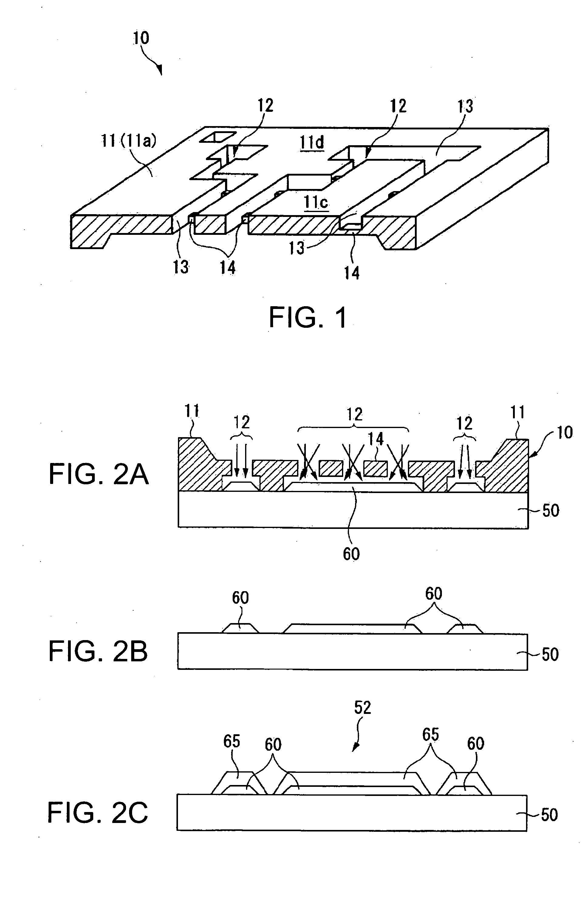
[0032] Next, a method of forming a pattern of the metal wiring 52 on a glass substrate 50 by using the mask 10 is described.

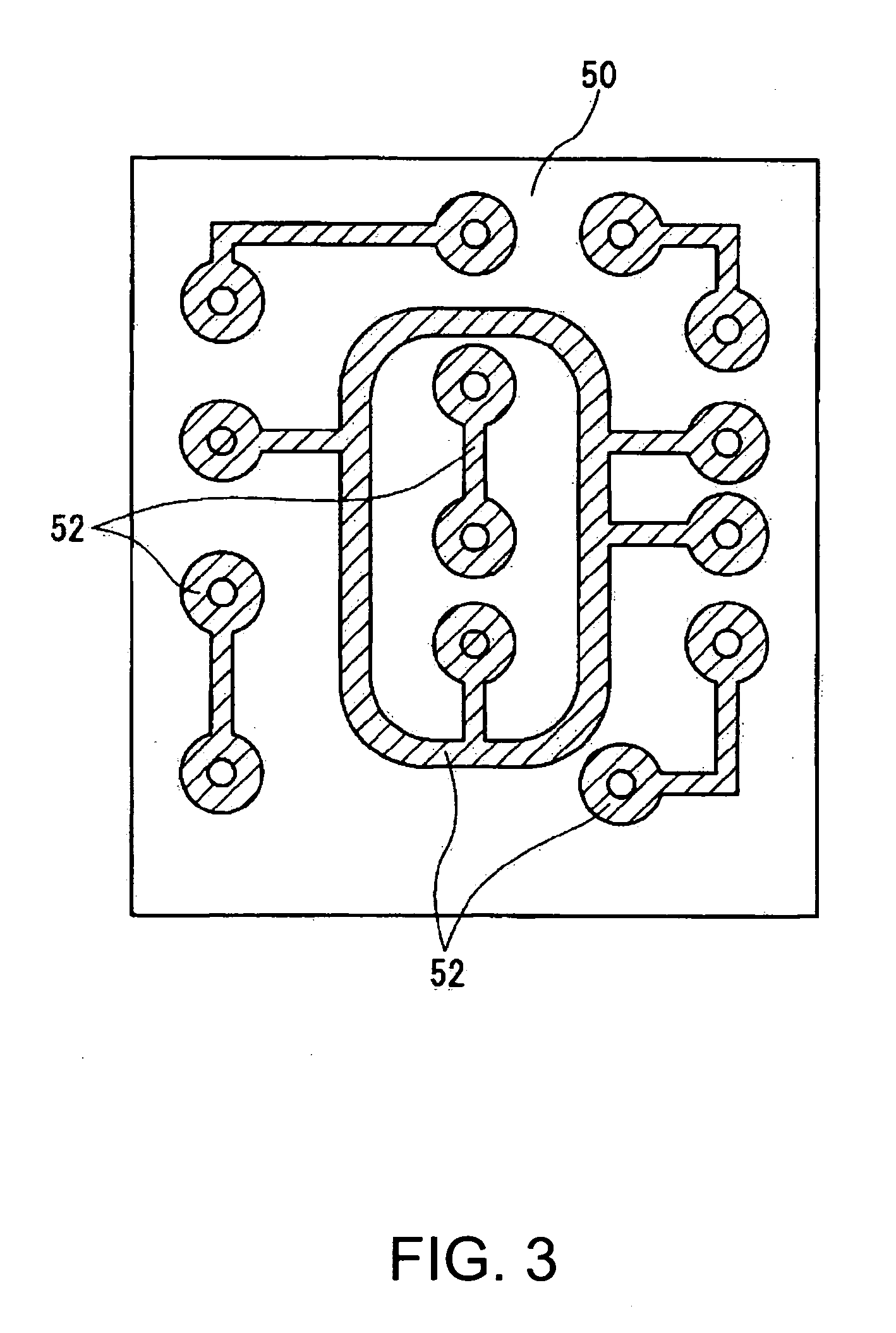
[0033]FIG. 2 shows a process for forming the electrical wiring 52 by using the mask 10. FIG. 3 shows the electrical wiring 52 formed by the process.

[0034] A substrate for forming the metal wiring 52 is not limited to a glass substrate 10 and other substrates may be used including a plastic substrate or a silicon substrate.

[0035] First, a metal base layer 60 is formed on the substrate 50 using the mask 10 by physical vapor-phase deposition such as evaporation and sputtering or a vapor-phase deposition such as CVD. The material of the metal base layer 60 is preferably gold or nickel. The following example is a case when nickel is used.

[0036] In detail, as shown in FIG. 2A, the surface 11a of the mask 10 is tightly attached to the glass substrate 50. Then, the metal base layer 60 made of nickel is formed by physical vapor-phase deposition...

second embodiment

A Film Forming Method

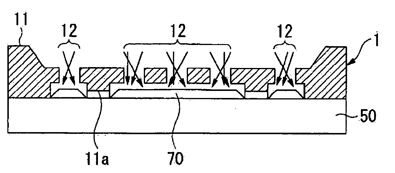
[0047] Next, a case of using aluminum as a metal base layer 70 is explained in a method of forming a pattern of a metal wiring 54 on the glass substrate 50 by using the mask 10.

[0048]FIGS. 4A to 4E are sequential steps of forming the metal wiring 54.

[0049] As shown in FIG. 4A, when aluminum film is formed as the metal base layer 70, the metal base layer 70 is formed on the glass substrate 50 with the mask 10 by an evaporation method, a physical vapor-phase growth method such as sputtering and a physical chemical vapor-phase growth method such as CVD. The thickness of the metal base layer 70 made of aluminum is preferably about 700 nm. Here, in order to form the metal film 70 made of aluminum, an oxide film formed on the surface must be removed to yield the metal film 70 made of aluminum having a thickness of around 100 nm, which is thicker than the metal film made of nickel.

[0050] The material for forming the metal base layer 70 may be an aluminum alloy. For...


PUM

PropertyMeasurementUnit
widthaaaaaaaaaa
distanceaaaaaaaaaa
thicknessaaaaaaaaaa

Abstract

A film forming method for forming a thin film pattern on a substrate, comprising a) forming the pattern of a metal base layer on the substrate by vapor-phase deposition with a mask; and b) forming a second metal film on the pattern of the metal base layer by plating the substrate.

Description

RELATED APPLICATIONS [0001] This application claims priority to Japanese Patent Application No. 2004-270891 filed Sep. 17, 2004 which is hereby expressly incorporated by reference herein in its entirety. BACKGROUND [0002] 1. Technical Field [0003] The present invention relates to a mask for forming wiring patterns on a substrate by a vapor-phase deposition method and the like. [0004] 2. Related Art [0005] Photolithography, dry etching and wet etching have been conventionally used for forming electric wiring on a substrate. These processes, however, need highly expensive facilities which increase product costs due to management expenses for plural processes and yield effects. Further, these processes consume a large amount of resist, development liquid, liquid for removing resist, and liquid or gas for etching. Hence, as shown in Japanese Unexamined Published Patent 4-236758, it is suggested to form a given wiring pattern on a substrate by forming a film with vapor-phase deposition i...

Claims


Application Information

Patent Timeline
Patent Type & Authority Applications(United States)
IPC IPC(8): B32B15/00B32B3/00B32B15/20
CPCH01L51/56H05K3/143Y10T428/12882H05K2201/0347Y10T428/24917H05K3/244H10K71/00H05K3/146
Inventor YOTSUYA, SHINICHIYODA, TSUYOSHIAKAGAWA, SUGURU
Owner SEIKO EPSON CORP
Why Eureka
Try Eureka