Semiconductor device
- Summary
- Abstract
- Description
- Claims
- Application Information
AI Technical Summary
Benefits of technology
Problems solved by technology
Method used
Image

Examples
embodiment 1
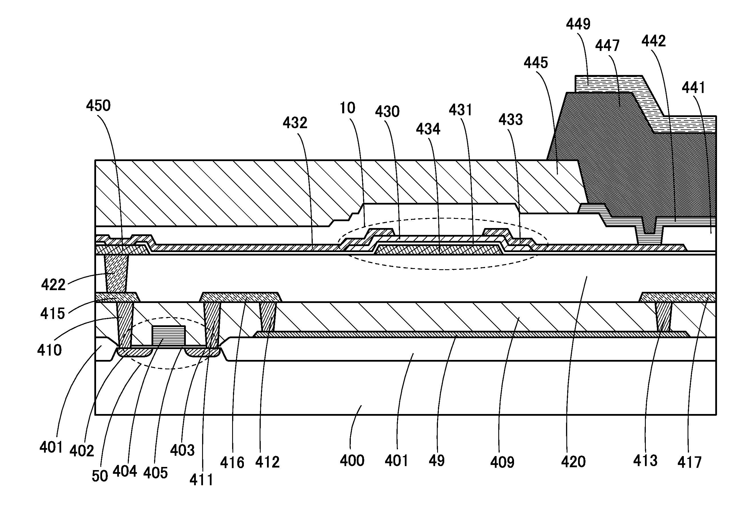
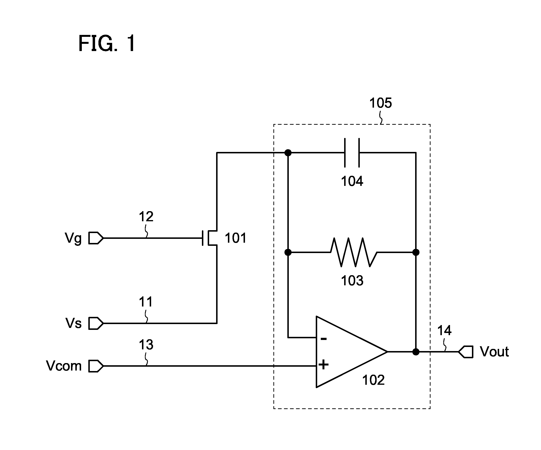
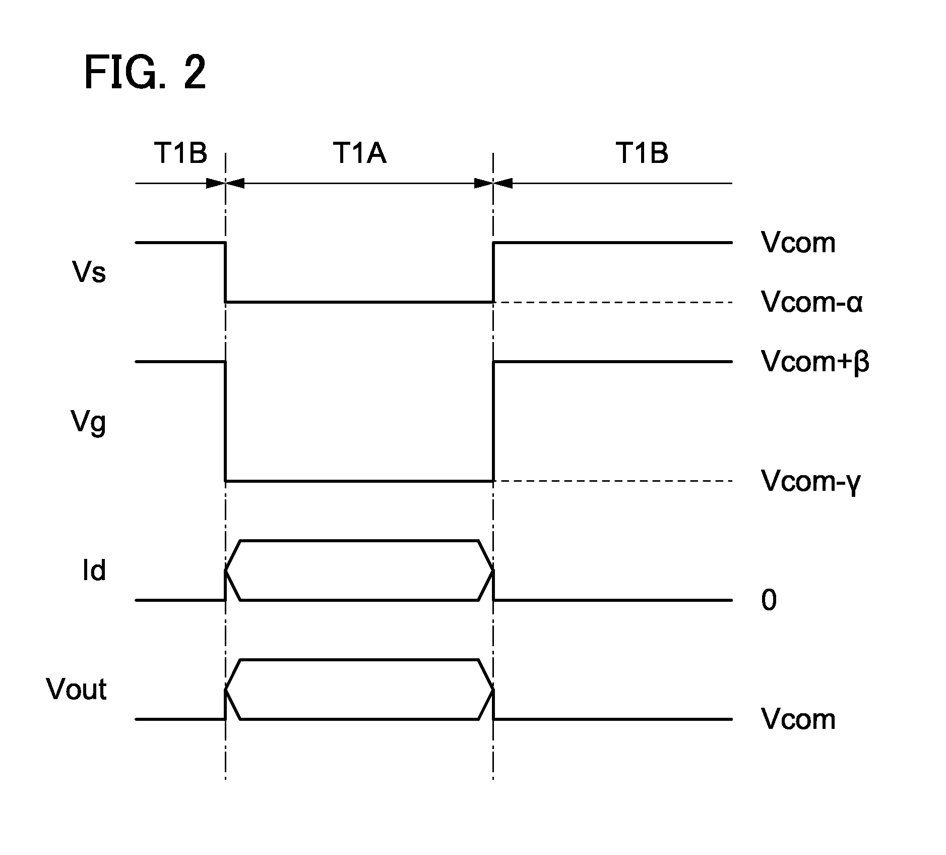
[0045]In this embodiment, a sensor circuit (also referred to as a semiconductor device) of one embodiment of the present invention will be described.
[0046]First, a configuration example of a sensor circuit in this embodiment will be described with reference to FIG. 1. FIG. 1 is an example of a circuit diagram of the sensor circuit.
[0047]The sensor circuit in FIG. 1 includes a transistor 101, an operational amplifier 102, a resistor 103, and a capacitor 104. A first terminal of the transistor 101 is connected to a wiring 11. A gate of the transistor 101 is connected to a wiring 12. A first input terminal (non-inverting input terminal) of the operational amplifier 102 is connected to a wiring 13. A second input terminal (inverting input terminal) of the operational amplifier 102 is connected to a second terminal of the transistor 101. An output terminal of the operational amplifier 102 is connected to a wiring 14. A first terminal of the resistor 103 is connected to the second input t...
embodiment 2
[0078]In this embodiment, a sensor circuit of one embodiment of the present invention will be described.
[0079]First, a configuration example of a sensor circuit in this embodiment will be described with reference to FIG. 3. FIG. 3 is an example of a circuit diagram of the sensor circuit.
[0080]The sensor circuit in FIG. 3 includes a transistor 201, a switch 202, a switch 203, a switch 204, a capacitor 205, a transistor 206, and the circuit 105. A first terminal of the transistor 201 is connected to the circuit 105. A first terminal of the switch 202 is connected to a wiring 21. A second terminal of the switch 202 is connected to a gate of the transistor 201. A first terminal of the switch 203 is connected to a wiring 22. A first terminal of the switch 204 is connected to the gate of the transistor 201. A second terminal of the switch 204 is connected to a second terminal of the switch 203. A first terminal of the capacitor 205 is connected to the second terminal of the switch 203. A ...
embodiment 3
[0106]In this embodiment, a sensor circuit of one embodiment of the present invention will be described.
[0107]First, a configuration example of a sensor circuit in this embodiment will be described with reference to FIG. 5. FIG. 5 is an example of a circuit diagram of the sensor circuit.
[0108]The sensor circuit in FIG. 5 includes a circuit 300, a transistor 301, and a resistor 302. A first terminal of the transistor 301 is connected to a wiring 31. A gate of the transistor 301 is connected to a wiring 32. A first terminal of the resistor 302 is connected to a wiring 33. A second terminal of the resistor 302 is connected to a second terminal of the transistor 301. An input terminal of the circuit 300 is connected to the second terminal of the transistor 301. An output terminal of the circuit 300 is connected to a wiring 34.
[0109]A portion where the input terminal of the circuit 300, the second terminal of the transistor 301, and the second terminal of the resistor 302 are connected i...
PUM
 Abstract
Description
Claims
Application Information
 - R&D
- Intellectual Property
- Life Sciences
- Materials
- Tech Scout
- Unparalleled Data Quality
- Higher Quality Content
- 60% Fewer Hallucinations
Browse by: Latest US Patents, China's latest patents, Technical Efficacy Thesaurus, Application Domain, Technology Topic, Popular Technical Reports.
© 2025 PatSnap. All rights reserved.Legal|Privacy policy|Modern Slavery Act Transparency Statement|Sitemap|About US| Contact US: help@patsnap.com