Multilayer Ceramic Electronic Component

a technology of electronic components and ceramics, applied in the direction of variable capacitors, fixed capacitor details, stacked capacitors, etc., can solve the problems of internal stress caused by the difference in thermal expansion coefficient, cracks to occur in response, increase in delamination, etc., to improve the resistance to thermal shock, improve the effect of continuity and small siz

Active Publication Date: 2015-03-19
MURATA MFG CO LTD
View PDF7 Cites 2 Cited by
  • Summary
  • Abstract
  • Description
  • Claims
  • Application Information

AI Technical Summary

Benefits of technology

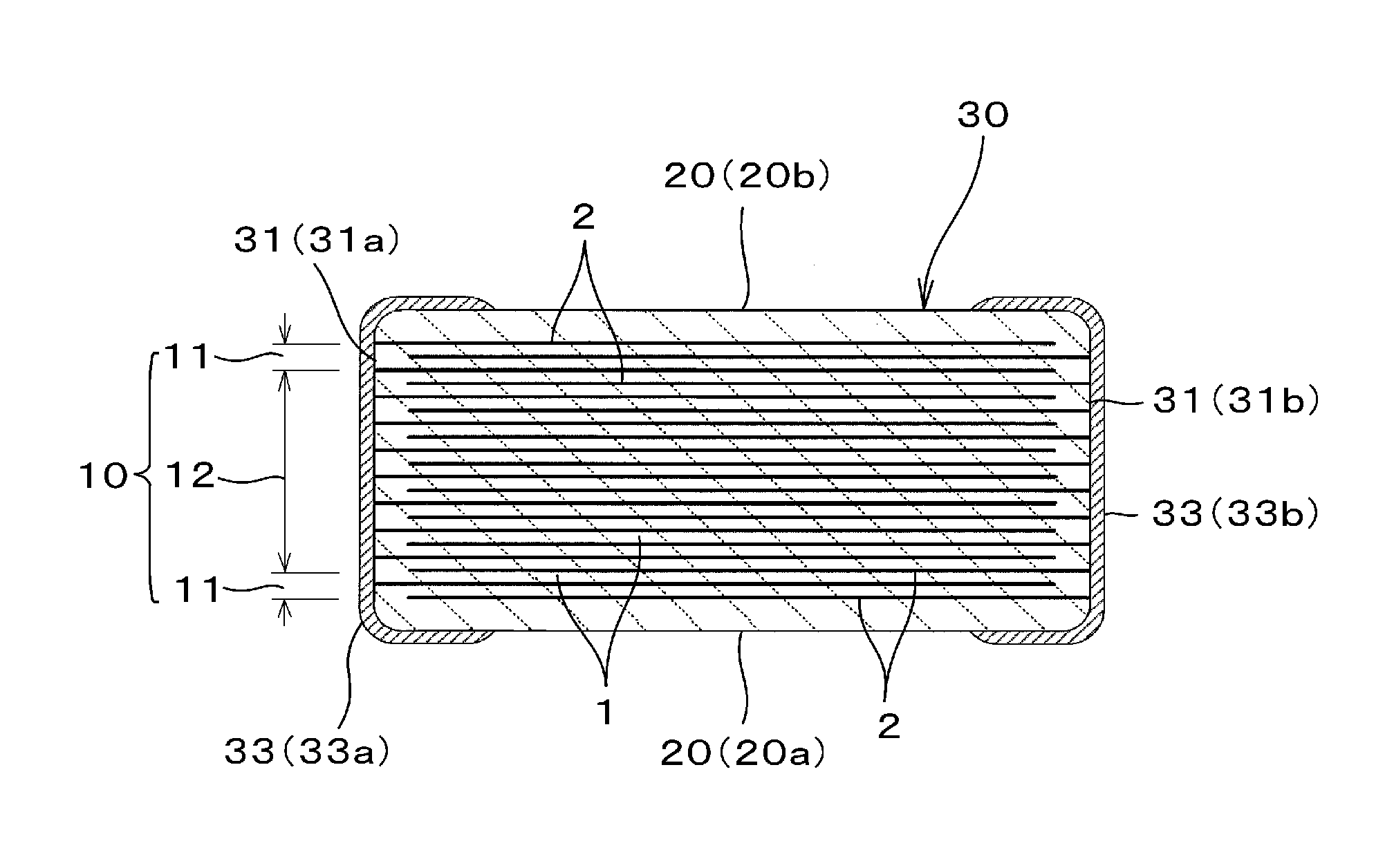
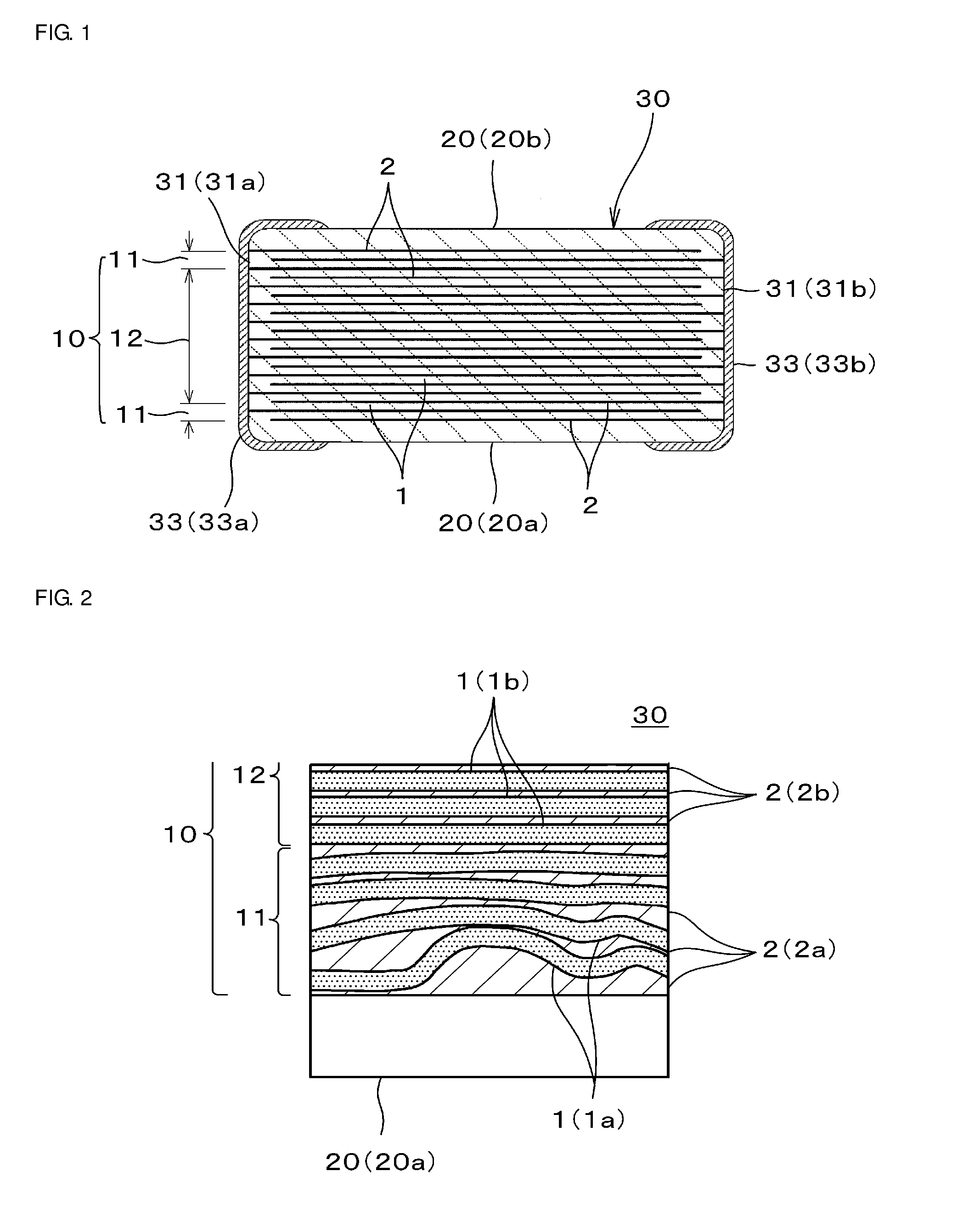
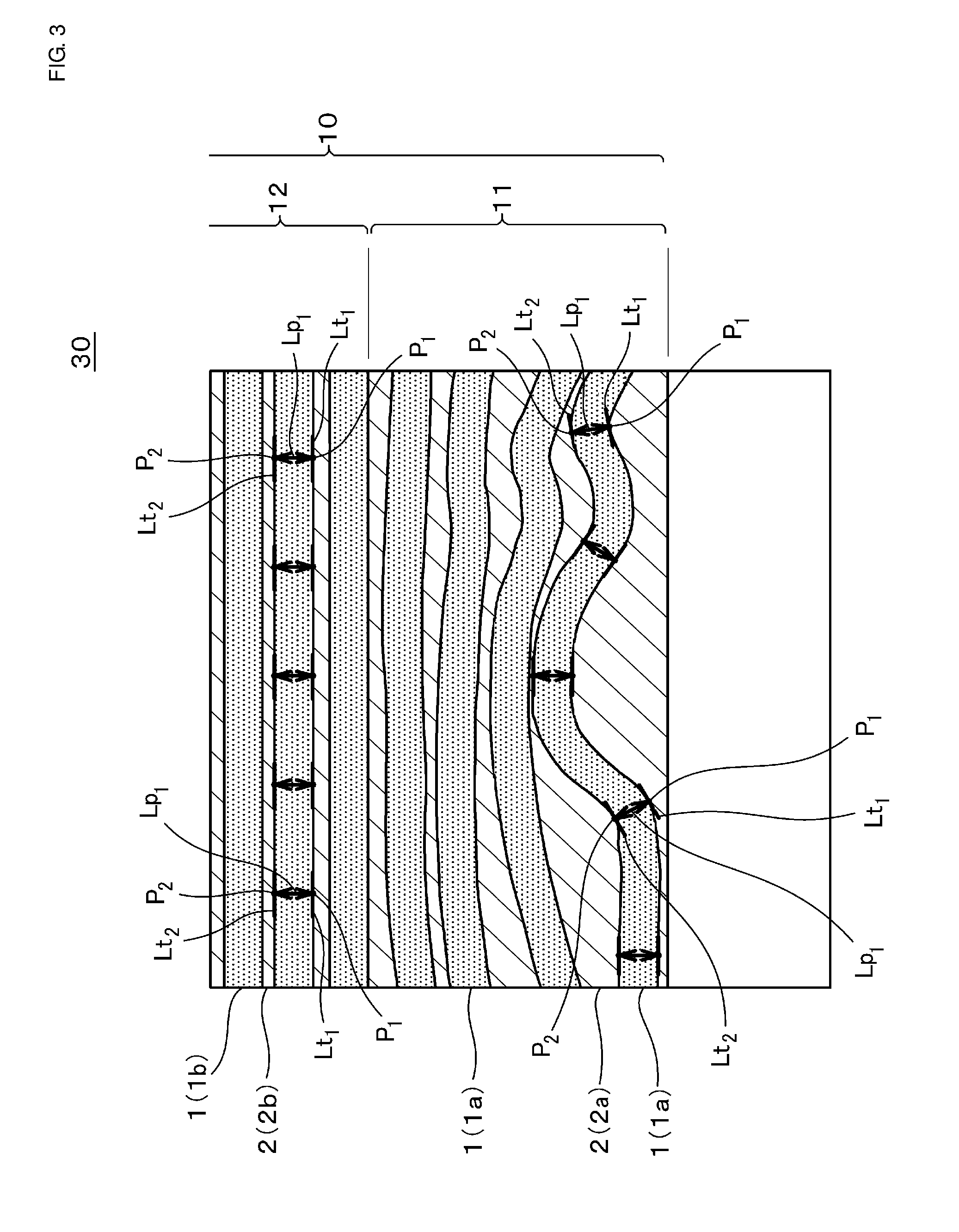
[0022]This allows efficient distribution of thermal shock and improves resistance to thermal shock.
[0023]Also, in both the thermal-shock absorbing portion and the normal multilayer portion, the inner electrode layers have high continuity and have no breaks. Therefore, for example, when the multilayer ceramic electronic component is a multilayer ceramic capacitor, a high-performance multilayer ceramic electronic component having a small size and a large electrostatic capacity can be obtained.

Problems solved by technology

As a result, a difference in sintering shrinkage temperature between the ceramic layers and the inner electrode layers leads to an increased occurrence of delamination.
This means that in a multilayer ceramic capacitor obtained through a sintering process, there is internal stress caused by the difference in thermal expansion coefficient.
This may cause cracks to occur in response to thermal shock.
If the multilayer ceramic electronic component is a multilayer ceramic capacitor, this leads to degradation of electrostatic capacity and failure to meet the demand for increased capacity.
A similar problem also applies to multilayer ceramic electronic components other than multilayer ceramic capacitors.

Method used


Image

  • Multilayer Ceramic Electronic Component
  • Multilayer Ceramic Electronic Component
  • Multilayer Ceramic Electronic Component

Examples


example

[0097]In Example, chip-type multilayer ceramic capacitors were produced as multilayer ceramic electronic components, and the relationship between the sintering temperature rise rate in the sintering process, the structure of the multilayer portion, the occurrence rate of cracks in the thermal shock test, and the electrostatic capacity was examined.

[0098](A) Preparation of Ceramic Base Powder for Ceramic Layers (Dielectric Layers)

[0099]Base powder (ceramic base powder) for ceramic layers serving as dielectric layers was prepared in the following procedure.

[0100]First, BaCO3 powder and TiO2 powder were weighed such that the ratio of Ba to Ti (Ba / Ti) was 1.001. These powders were wet-ground and mixed in a zirconia ball mill.

[0101]After being dried, the powder mixture was heated to 900° C. or more and subjected to heat treatment (calcination), which produced a perovskite-type compound oxide (BaTiO3 ceramic powder) having an average particle diameter of 0.20 μm.

[0102]Then 0.6 mol parts o...


PUM

PropertyMeasurementUnit
particle diameteraaaaaaaaaa
widthaaaaaaaaaa

Abstract

A multilayer ceramic electronic component that has a multilayer portion having an outer layer portion adjacent region including an area in contact with an outer layer portion that forms a thermal-shock absorbing portion that includes curved ceramic layers and inner electrode layers smoothly varying in thickness from point to point. A region to an inside of the thermal-shock absorbing portion forms a normal multilayer portion that includes ceramic layers with less curvature than the ceramic layers in the thermal-shock absorbing portion and inner electrode layers with less variation in thickness from point to point in a direction along a principal surface of the outer layer portion than the inner electrode layers in the thermal-shock absorbing portion.

Description

CROSS REFERENCE TO RELATED APPLICATIONS[0001]The present application is a continuation of International application No. PCT / JP2013 / 062553, filed Apr. 30, 2013, which claims priority to Japanese Patent Application No. 2012-118242, filed May 24, 2012, the entire contents of each of which are incorporated herein by reference.FIELD OF THE INVENTION[0002]The present invention relates to a multilayer ceramic electronic component that includes a multilayer portion having a plurality of stacked ceramic layers and inner electrode layers each interposed between adjacent ceramic layers, and an outer layer portion having no inner electrode layers, formed by one or more ceramic layers, and disposed such that the multilayer portion is sandwiched from both principal surfaces.BACKGROUND OF THE INVENTION[0003]A chip-type multilayer ceramic capacitor is one of typical multilayer ceramic electronic components. With miniaturization and sophistication of electronic devices in recent years, there is more...

Claims


Application Information

Patent Timeline
Patent Type & Authority Applications(United States)
IPC IPC(8): H01G4/258H01G4/30
CPCH01G4/30H01G4/258H01C7/1006H01C7/102H01C7/18H01G4/012H01G4/12
Inventor WADA, HIROYUKIHIRATA, YOSUKEHIRAMATSU, TAKASHISAITO, YOSHITOTSUJI, HIDEAKIUKAI, HIROYUKI
Owner MURATA MFG CO LTD
Why Eureka
Try Eureka