Check patentability & draft patents in minutes with Patsnap Eureka AI!

Ultralow power carbon nanotube logic circuits and method of making same

Active Publication Date: 2015-04-16
RGT UNIV OF MINNESOTA +1
View PDF10 Cites 16 Cited by
  • Summary
  • Abstract
  • Description
  • Claims
  • Application Information

AI Technical Summary

Benefits of technology

The patent text describes a CMOS logic device that uses single-walled carbon nanotubes (SWCNTs) to form logic circuits. The device includes both PMOS and NMOS transistors, with a local metallic gate structure formed of metal. The transistors are chemically doped with benzyl viologen. The device has a low noise margin of 0.32 VDD and a high noise margin of 0.54 VDD. The device can be used as a logic inverter or a logic NAND gate. The transistors are covered with encapsulation layers made of photoresist or Al2O3. The device has a static power consumption of less than about 100 nW in a static state and a peak power consumption of about 10 nW in a transfer state.

Problems solved by technology

However, power consumption during operation of the transistors is a significant issue.
However, previous studies have not addressed any transistors or logic circuits with satisfactory ultralow power consumption.
Therefore, a heretofore unaddressed need exists in the art to address the aforementioned deficiencies and inadequacies.

Method used


Image

  • Ultralow power carbon nanotube logic circuits and method of making same
  • Ultralow power carbon nanotube logic circuits and method of making same
  • Ultralow power carbon nanotube logic circuits and method of making same

Examples


example one

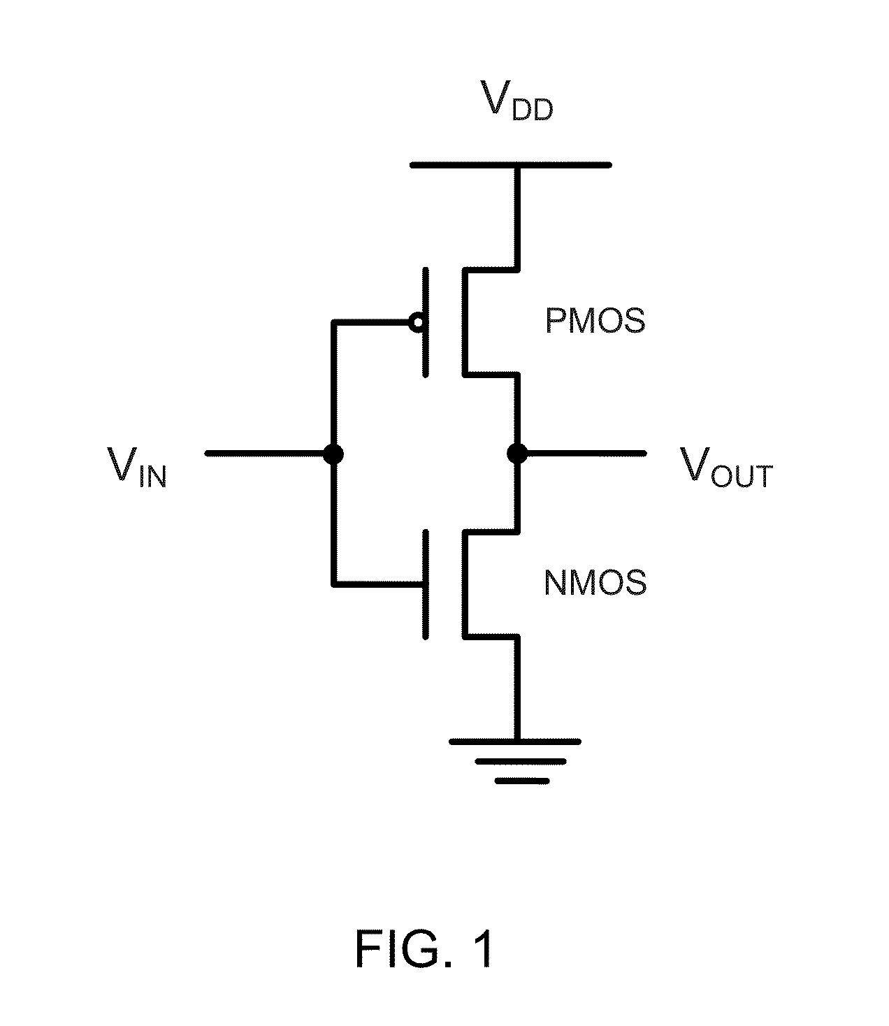
[0076]In one embodiment, threshold voltage control is demonstrated for both p-type and n-type SWCNT TFTs via a local Ni gate structure, which enables ultralow power complementary device operation. For example, a high-performance SWCNT CMOS inverter (logic NOT gate) is provided with reference to FIG. 1 as an initial illustration of this device architecture.

[0077]FIG. 1 shows schematically a circuit diagram of a CMOS logic inverter according to certain embodiments of the disclosure. As shown in FIG. 1, the CMOS logic inverter includes a p-type MOS (PMOS) transistor and an n-type MOS (NMOS) transistor. Each of the PMOS and NMOS transistors has a gate, a source and a drain. As shown in FIG. 1, the gate of the PMOS transistor and the gate of the NMOS transistor are respectively electrically connected to a common input voltage line for alternatively receiving a common input voltage VIN. The drain of the first PMOS transistor and the drain of the NMOS transistor are respectively electrical...

example two

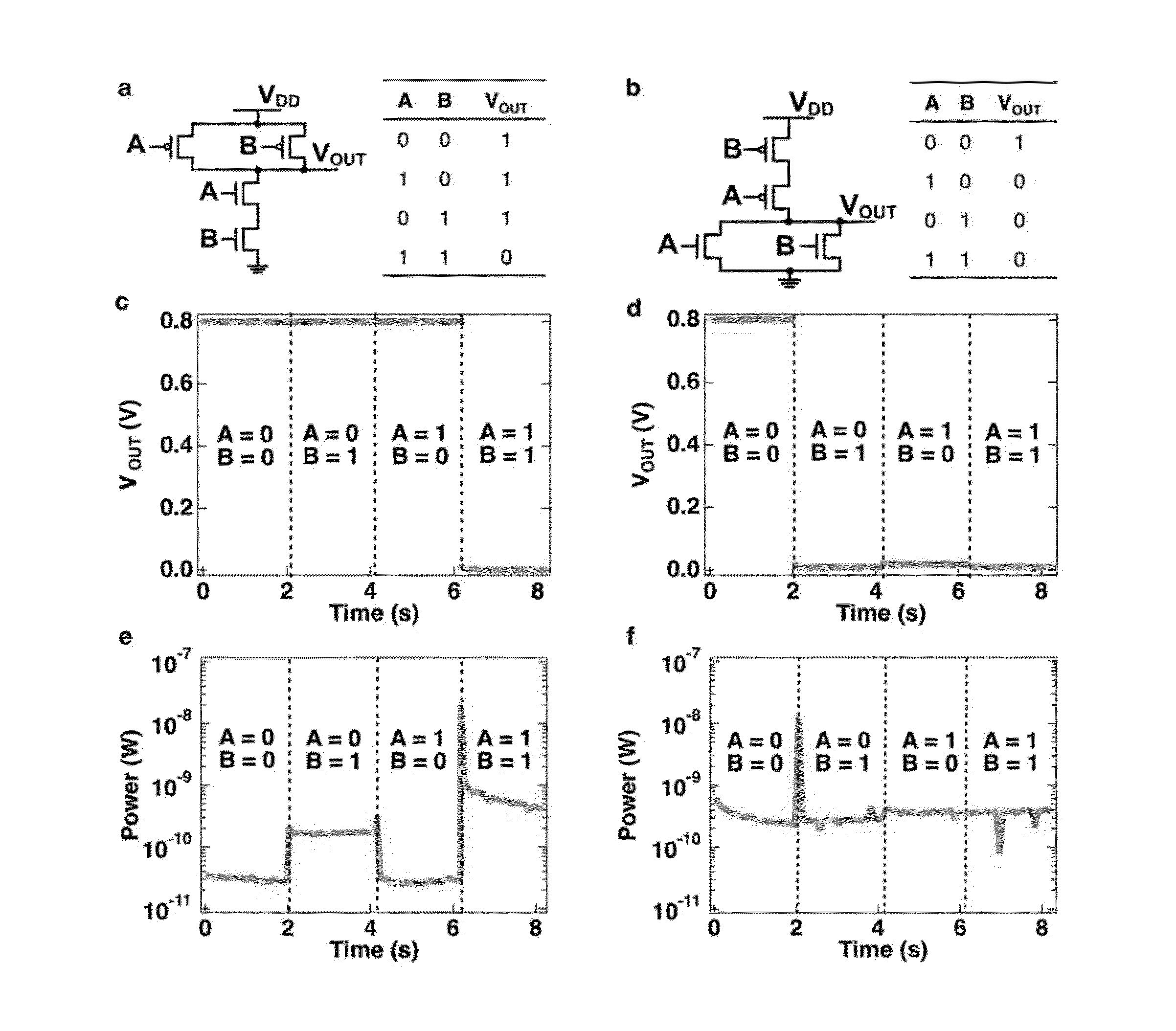
[0083]To demonstrate the next level of CMOS integration, NAND and NOR logic gates were fabricated. FIG. 9 shows the two-input CMOS NAND and NOR gate electrical characteristics according to certain embodiments of the disclosure, where (a) shows a CMOS logic NAND circuit diagram and associated truth table; (b) shows a CMOS logic NOR circuit diagram and associated truth table; (c) shows the output voltages (VOUT) for each possible two input state for the NAND circuit; (d) shows the output voltages (VOUT) for each possible two input state for the NOR circuit; (e) shows NAND power consumption for each possible two input state; and (f) shows NOR power consumption for each possible two input state. The supply voltage (VDD) for the circuits is 0.8 V. Input voltages of 0 V (GND) and 0.8 V (VDD) are treated as logic “0” and “1”, respectively.

[0084]As shown in FIG. 9(a), a logic NAND gate is realized by connecting two n-type TFTs in series and two p-type TFTs in parallel. Specifically, the NAN...

example three

1. Preparation of Benzyl Viologen Solution for n-Type Single-Walled Carbon Nanotube Transistors

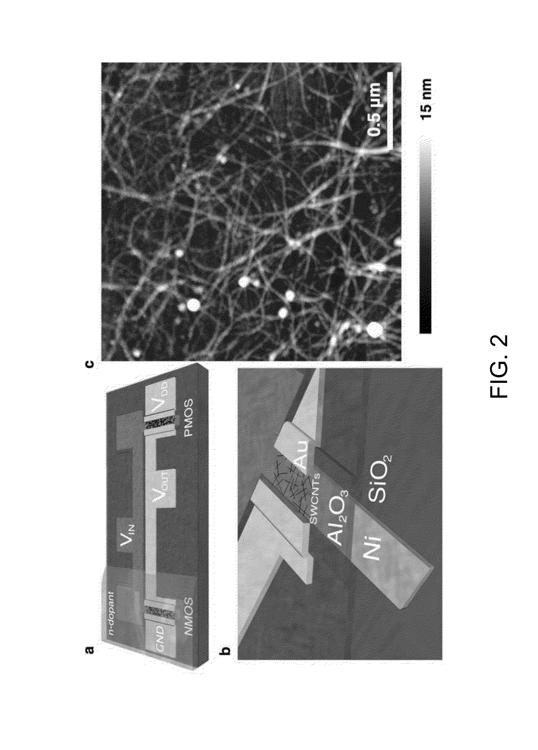
[0088]In certain embodiments, benzyl viologen dichloride (0.1 g; 97%, Aldrich) was dissolved in 5 mL of deionized water, after which 2 mL of toluene (>99.5%, Sigma Aldrich) was added on top of the water solution, creating a biphasic solution. Next, 1 mL of sodium borohydride (>98% Aldrich) in water (200 mM) was added as a catalytic reducing agent, causing the benzyl viologen solution to turn purple and evolve H2 gas. The biphasic solution was left standing overnight, and the toluene containing ˜10 mM benzyl viologen was decanted (as shown in FIG. 3) and used for n-type doping for all n-type transistors.

2. Dispersion and Separation of SWCNTs

[0089]In certain embodiments, 45 mg of single-walled carbon nanotubes (SWCNTs) synthesized by the arc discharge method (P2, Carbon Solutions) were added to 6.6 mL of 1% w / v aqueous sodium cholate (SC) solution. This mixture was then sonicated for 60 min ...


PUM


Abstract

In one embodiment, a complementary metal-oxide-semiconductor (CMOS) logic device formed with single-walled carbon nanotubes (SWCNTs) includes: at least one p-type metal-oxide-semiconductor (PMOS) thin-film transistor (TFT) formed with the SWCNTs, and at least one n-type metal-oxide-semiconductor (NMOS) TFT formed with the SWCNTs, where each of the at least one PMOS TFT and the at least one NMOS TFT has a gate, a source and a drain. The gate of each of the at least one PMOS TFT and the gate of each of the at least one NMOS TFT is configured to alternatively receive at least one input voltage, and respectively includes a local metallic gate structure formed of a metal. At least one of the drain of the at least one PMOS TFT and the drain of the at least one NMOS TFT is configured to output an output voltage VOUT.

Description

CROSS-REFERENCE TO RELATED PATENT APPLICATION[0001]This application claims priority to and the benefit of, pursuant to 35 U.S.C. §119(e), U.S. provisional patent application Ser. No. 61 / 889,841, filed Oct. 11, 2013, entitled “ULTRALOW POWER CARBON NANOTUBE LOGIC CIRCUITS,” by Mark C. Hersam, Michael L. Geier, Pradyumna L. Prabhumirashi, Weichao Xu and Hyungil Kim, which is incorporated herein in its entirety by reference.[0002]Some references, which may include patents, patent applications and various publications, are cited and discussed in the description of this invention. The citation and / or discussion of such references is provided merely to clarify the description of the present invention and is not an admission that any such reference is “prior art” to the invention described herein. All references cited and discussed in this specification are incorporated herein by reference in their entireties and to the same extent as if each reference was individually incorporated by refe...

Claims


Application Information

Patent Timeline
IPC IPC(8): H01L27/12H01L27/092H01L29/06H01L29/16H01L29/786H01L21/324H01L29/49H01L23/31H01L23/29H01L21/02H01L21/56H03K19/0948H01L29/167
CPCH01L27/1222H03K19/0948H01L27/0922H01L27/1259H01L27/127H01L29/0673H01L29/16H01L29/78684H01L29/78696H01L29/167H01L29/495H01L23/3135H01L23/291H01L23/293H01L21/02178H01L21/56H01L21/02527H01L21/02606H01L21/324H01L2924/0002H03K19/215H10K85/221H10K10/484H01L2924/00H10K19/10H10K10/88H10K10/466H10K10/472H10K10/481H10K71/15H10K71/40H10K71/231H10K71/621H10K2102/00
Inventor HERSAM, MARK C.GEIER, MICHAEL L.PRABHUMIRASHI, PRADYUMNA L.XU, WEICHAOKIM, HYUNGIL
Owner RGT UNIV OF MINNESOTA
Features
  • R&D
  • Intellectual Property
  • Life Sciences
  • Materials
  • Tech Scout
  • Unparalleled Data Quality
  • Higher Quality Content
  • 60% Fewer Hallucinations
Learn More