Plasma processing apparatus and method therefor

a technology of plasma processing and processing apparatus, which is applied in the direction of cleaning process and apparatus, chemistry apparatus and processes, electric discharge tubes, etc., can solve the problems of resist damage to the outer peripheral part of the substrate, holding sheet, and frame, and achieve the effect of improving plasma processing performance and electrostatic attraction performan

Active Publication Date: 2015-05-07
PANASONIC INTELLECTUAL PROPERTY MANAGEMENT CO LTD
View PDF2 Cites 20 Cited by
  • Summary
  • Abstract
  • Description
  • Claims
  • Application Information

AI Technical Summary

Benefits of technology

[0008]The present invention has an object to improve both the plasma process performance and the electrostatic attraction performance in a plasma processing apparatus for plasma-processing the substrate held by the carrier.
[0012]The substrate is electrostatically attracted by the first electrostatic attraction electrode of unipolar type. A electrostatic attraction force of the unipolar-type electrostatic attraction electrode is weaker than that of the bipolar-type. However, the unipolar-type electrostatic attraction electrode is superior to the bipolar-type in term of the plasma processing performance due to that a whole surface of the substrate can be equally attracted. For example, in the case of plasma dicing, both the attraction force fluctuation of the before and after of singulating the substrate and the difference of the localized attraction force of unipolar type are less than those of bipolar type. In addition, specifically, in the case of the process (Si etching process, for example) where the radical reaction of the high plasma density and the low bias power are dominant, with the change of the bias power of the before and after of singulating the substrate, the pattern of the electrostatic attraction electrode of bipolar type may be transcribed to the substrate side. On the other hand, the frame and the holding sheet (between the substrate and the frame) are electrostatically attracted to the electrode unit by the second electrostatic attraction electrode of bipolar type. The electrostatic attraction electrode of bipolar type is inferior to that of unipolar type in terms of the plasma process performance, but is stronger than that of unipolar type in terms of the electrostatic attraction force. That is, in the present invention, the first electrostatic attraction electrode of unipolar type is used for the electrostatic attraction of the substrate which directly influences the plasma process performance, on the other hand, the second electrostatic attraction electrode of bipolar type with the strong electrostatic attraction force is used for the frame and the holding sheet with less influence on the plasma process performance than the substrate. As a result, both the plasma process performance and the electrostatic attraction performance can be improved. With the improvement of the electrostatic attraction performance, the holding sheet and the frame are cooled effectively by the heat transfer to the stage, and the damage caused by the radiant heat from the cover can be reduced effectively.
[0017]According to the invention, the first electrostatic attraction electrode of unipolar type is used for the electrostatic attraction of the substrate, whereas the second electrostatic attraction electrode of bipolar type is used for the electrostatic attraction of the frame and the holding sheet. This improves both of plasma processing performance and electrostatic attraction performance.

Problems solved by technology

Radiant heat from the heated cover gives thermal damage to the resist of the substrate outer peripheral part, holding sheet, and frame.

Method used


Image

  • Plasma processing apparatus and method therefor
  • Plasma processing apparatus and method therefor
  • Plasma processing apparatus and method therefor

Examples


first embodiment

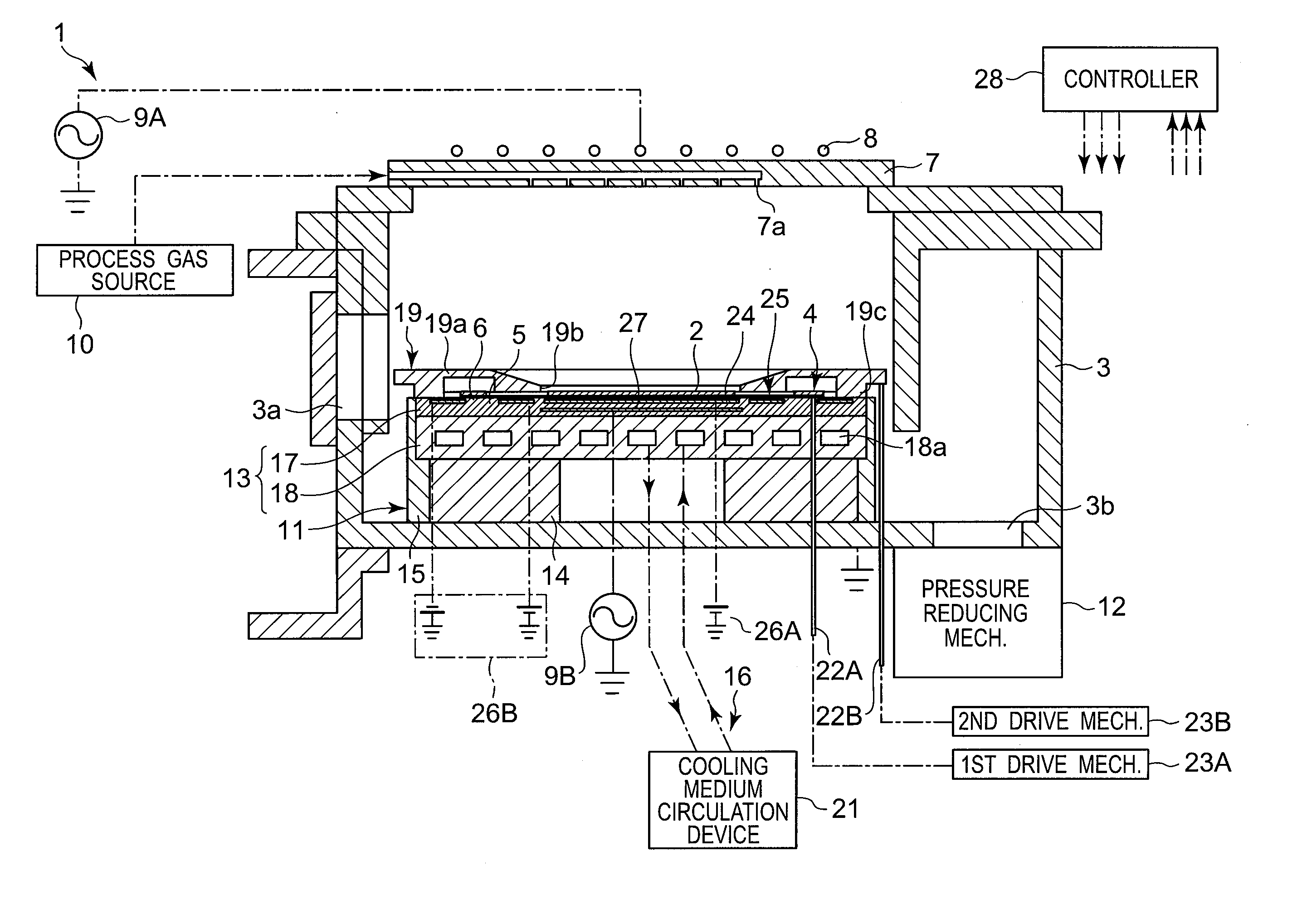
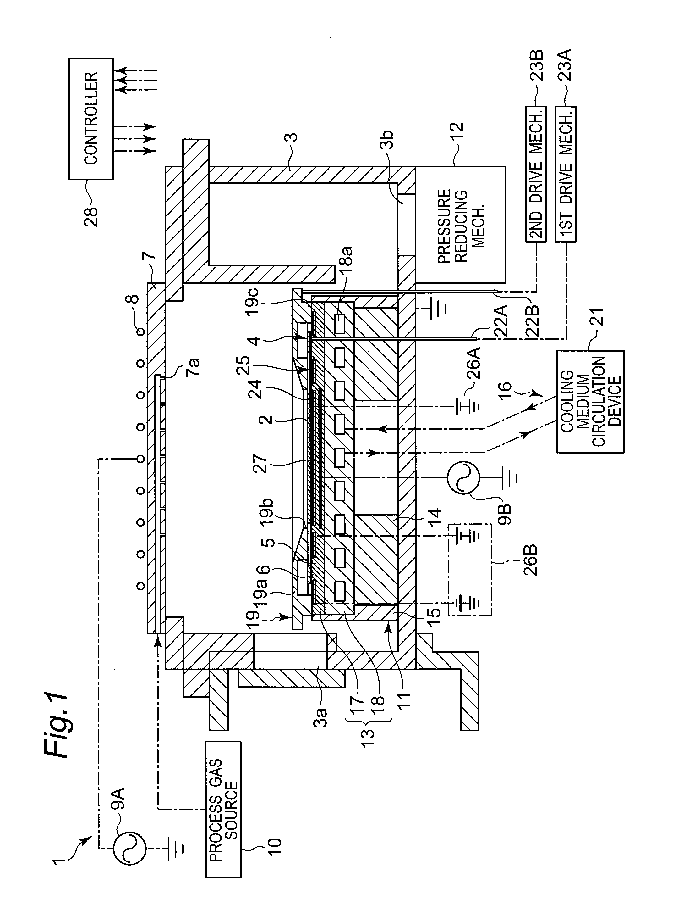
[0027]FIGS. 1 to 4 show a dry etching apparatus 1 which is an example of a plasma processing apparatus according to an embodiment of the present invention. In this embodiment, plasma dicing is performed on a wafer (substrate) 2 by this dry etching apparatus 1. Plasma dicing is a method of cutting, by using a dry etching boundary line (street), the wafer 2 in which a plurality of IC units (semiconductor devices) are formed, and dividing the wafer 2 into individual IC units. Referring to FIG. 2, the wafer 2 having a circular shape in this embodiment includes a front face 2a on which IC units, etc., not shown in the figure, are formed, and a back face 2b (on which IC units, etc. are not formed) on the opposite side of the front face 2a. On the front face 2a of the wafer 2, a mask (not shown in the figure) is formed in a pattern for plasma dicing.

[0028]Referring to FIG. 1, the dry etching apparatus 1 includes a chamber (vacuum vessel) 3 which has a pressure reducible internal space. A c...

second embodiment

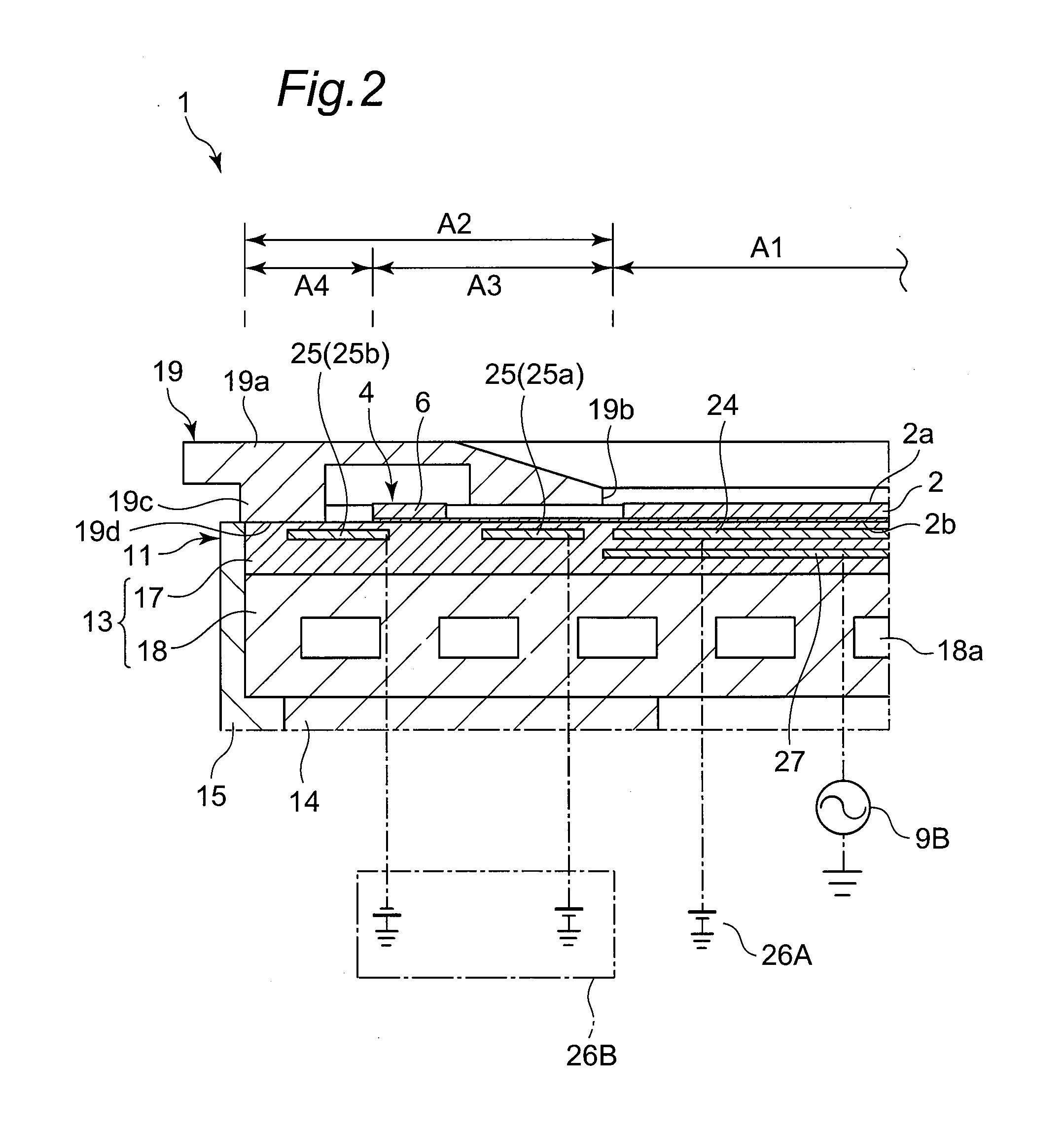
[0060]In the second embodiment shown in FIG. 6, the bias electrode 27 and the second radio frequency power source 9B are eliminated, and a voltage obtained by superimposing a radio frequency voltage as a bias voltage on a direct current voltage is applied from the power source 29 to the first electrostatic attraction electrode 24. By eliminating the second radio frequency power source 9B, the configuration of the electrostatic chuck 17 can be simplified.

third embodiment

[0061]In the third embodiment shown in FIG. 7, the second electrostatic attraction electrode 25 is disposed only in the area including the area in which the frame 6 is placed via the holding sheet 5 and the area in which the holding sheet 5 between the wafer 2 and the frame 6 is placed on the electrostatic chuck 17. In other words, the second electrostatic attraction electrode 25 is not disposed in the area (indicated by the reference sign A4 in FIG. 7) in which the cover 19 in the lowered position abuts onto the electrostatic chuck 17, and the cover 19 is not electrostatically attracted to the electrostatic chuck 17. During the plasma process, the cover 19 is urged to the stage 11 side by the second drive mechanism 23B, and whereby the contact face 19d of the annular protrusion portion 19c is pressed onto the upper face of the electrostatic chuck 17.

[0062]The present invention is not limited to the configurations in the embodiments, and various modifications are possible.

[0063]For ...


PUM

PropertyMeasurementUnit
outer diameteraaaaaaaaaa
pressureaaaaaaaaaa
areaaaaaaaaaaa

Abstract

A dry etching apparatus plasma processes a wafer held by a carrier having a frame and an holding sheet. A electrode unit of a stage includes an electrostatic chuck. Adjacent to an upper surface of the electrostatic chuck, a first electrostatic attraction electrode and a second electrostatic attraction electrode are incorporated. The first electrostatic attraction electrode is of unipolar type and electrostatically attracts the wafer via the holding sheet. The second electrostatic electrode is of bipolar type and electrostatically attracts the frame via the holding sheet as well as a holding sheet between the wafer and the frame. Both of plasma processing performance and electrostatic attraction performance are improved.

Description

CROSS-REFERENCE TO RELATED APPLICATIONS[0001]This application claims priority of Japanese Patent Application No. 2013-228097 filed on Nov. 1, 2013, the contents of which are incorporated herein by reference.BACKGROUND OF THE INVENTION[0002]1. Field of the Invention[0003]The present invention relates to a plasma processing apparatus and a method therefor.[0004]2. Description of Related Art[0005]The plasma processing apparatuses disclosed in Japanese Patent No. 4858395 and United States Patent Application Publication No. 2012 / 0238073 have process targets of a substrate (wafer, for example) held in a carrier including an annular frame and a holding sheet. The substrate is held on a holding sheet. In addition, these plasma processing apparatuses include a cover that covers a frame and an area between the substrate outer-periphery of the holding sheet and the frame so that the frame and the area are not to be exposed to the plasma.[0006]The cover is heated by being exposed to plasma, and...

Claims


Application Information

Patent Timeline
Patent Type & Authority Applications(United States)
IPC IPC(8): B08B7/00
CPCB08B7/0021H01J37/32568H01J37/32697H01J37/32715H01J37/32724H01L21/6831H01J37/3211H01J37/3244H01J37/32816H01J2237/002H01J2237/334H01L21/3065H01L21/67069H01L21/6833H01L21/78
Inventor OKITA, SHOGO
Owner PANASONIC INTELLECTUAL PROPERTY MANAGEMENT CO LTD
Why Eureka
Try Eureka