Laminated ceramic capacitor and method for manufacturing laminated ceramic capacitor

a technology of laminated ceramic capacitors and ceramic capacitors, which is applied in the manufacture of capacitors, fixed capacitor details, fixed capacitors, etc., can solve the problems of insufficient durability and achieve the effects of high reliability, high efficiency and high sn ra

Active Publication Date: 2015-06-04
MURATA MFG CO LTD
View PDF8 Cites 27 Cited by
  • Summary
  • Abstract
  • Description
  • Claims
  • Application Information

AI Technical Summary

Benefits of technology

[0041]forming an unfired ceramic laminated body including a plurality of unfired ceramic dielectric layers and a plurality of unfired internal electrode patterns formed by applying a conductive paste and provided along the plurality of interfaces between the unfired ceramic dielectric layers; and firing the unfired ceramic laminated body to obtain the ceramic laminated body, and uses, as the conductive paste, a conductive paste containing a Sn constituent blended common material with a Sn constituent blended in a ceramic material powder that has the same or substantially the same composition as that of the ceramic material powder constituting the unfired ceramic dielectric layers, thus making it possible to manufacture, with certainty, a highly reliable laminated ceramic capacitor which is configured so that the proportion of a region where the Sn / (Ni+Sn) ratio is 0.001 or more in terms of molar ratio is 75% or more in a region (near-interface region) of the internal electrode at a depth of 20 nm from the surface opposed to the ceramic dielectric layer, whereas the proportion of a region where the Sn / (Ni+Sn) ratio is 0.001 or more in terms of molar ratio is less than 40% in a central region (inner electrode region) in the thickness direction of the internal electrode, that is, a higher rate of Sn is present in the near-interface region of the internal electrode than in the inner electrode region, capable of achieving high electrostatic capacitance, and excellent in high-temperature load life.
[0042]In the method for manufacturing a laminated ceramic capacitor according to the present invention, the conductive paste containing the Sn constituent blended common material with the Sn constituent blended in a ceramic material powder that has the same or substantially the same composition as that of the ceramic material powder constituting the unfired ceramic dielectric layers is used as the conductive paste as the conductive paste as described above. Thus, in the firing step, the common material (Sn constituent blended common material) is pulled to the high-affinity ceramic dielectric layer side, and the Sn constituent blended in the common material is also pulled to the ceramic dielectric layer side. As a result, it becomes possible to manufacture, with certainty, and moreover with great efficiency, a laminated ceramic capacitor which has the distinctive feature of a higher rate of Sn present in the interface (near-interface region) between the internal electrode and the ceramic dielectric layer than in the internal part (inner electrode region) of the internal electrode.
[0043]Furthermore, the laminated ceramic capacitor according to another aspect of the present invention is configured so that the internal electrodes contain Ni and Sn, and have a solid solution of Sn in Ni, the proportion of Sn to the total amount of Sn and Ni is 2 atomic % or more in a region of the internal electrode at a depth of 2 nm from the interface between the internal electrode and the ceramic dielectric layer; and the proportion of Sn to the total amount of Sn and Ni in a region of the internal electrode at a depth of 2 nm from the interface between the internal electrode and the ceramic dielectric layer is higher than the proportion of Sn in a region of the internal electrode at a depth of 20 nm or more from the interface between the internal electrode and the ceramic dielectric layer by 1.0 atomic % or more, thus making it possible to achieve high electrostatic capacitance, and to provide a highly reliable laminated ceramic capacitor which is excellent in high-temperature load life.
[0044]In the laminated ceramic capacitor according to another aspect of the present invention, the formation of the Ni—Sn alloy in the internal electrodes and the Sn proportion which meets the requirements mentioned above are believed to change the condition of the interface between the ceramic dielectric layer and the internal electrode, thereby providing an improvement in high-temperature load life. In particular, the presence of a lot of Ni—Sn alloy in the region of the internal electrode at a depth of 2 nm from the interface between the internal electrode and the ceramic dielectric layer is assumed to have an important part for the improvement in high-temperature load life.

Problems solved by technology

However, the laminated ceramic capacitor including the internal electrodes using Ni as a main constituent in Patent Document 1 has the problem of still insufficient durability in the case of high-voltage application for meeting the recent requirements of reduction in size and increase in capacitance.

Method used


Image

  • Laminated ceramic capacitor and method for manufacturing laminated ceramic capacitor
  • Laminated ceramic capacitor and method for manufacturing laminated ceramic capacitor
  • Laminated ceramic capacitor and method for manufacturing laminated ceramic capacitor

Examples


embodiment 1

[0053]

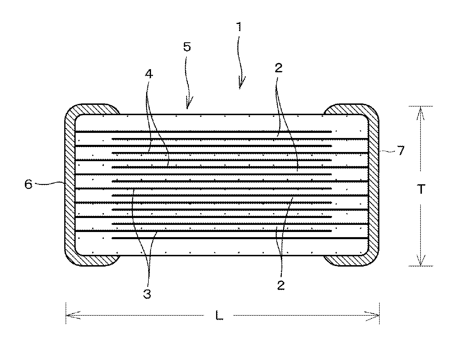
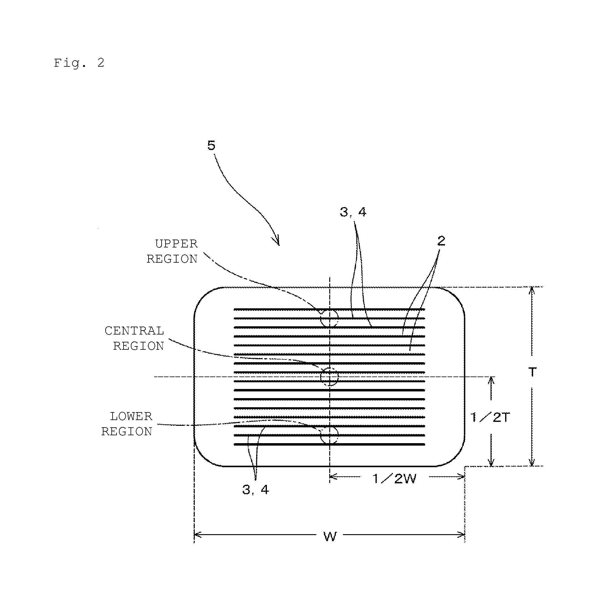
[0054]FIG. 1 is a front cross-sectional view illustrating the configuration of a laminated ceramic capacitor according to an embodiment (Embodiment 1) of the present invention.

[0055]This laminated ceramic capacitor 1 includes a ceramic laminated body 5. The ceramic laminated body 5 includes a plurality of ceramic dielectric layers 2 stacked, and a plurality of internal electrodes 3 and 4 provided therein to be opposed to each other with the ceramic dielectric layers 2 interposed therebetween. It is to be noted that the internal electrodes 3 and 4 provided in the ceramic dielectric layers 2 are alternately extracted to opposite end surfaces of the ceramic laminated body 5.

[0056]Further, on the end surfaces of the ceramic laminated body 5, which are opposed to each other, external electrodes 6 and 7 are provided so as to be electrically connected to the internal electrodes 3 and 4.

[0057]The external electrodes 6 and 7 are formed on the end surfaces opposed to each other on the o...

embodiment 2

[0118]Also in this Embodiment 2, a laminated ceramic capacitor configured in the same way as the laminated ceramic capacitor according to Embodiment 1 of the present invention was manufactured which was structured as shown in FIG. 1.

[0119]

[0120]Next, a method for manufacturing a laminated ceramic capacitor 1 according to Embodiment 2 of the present invention will be described.

[0121](1) First, predetermined amounts of BaCO3 powder and TiO2 powder were weighed as raw materials for a perovskite-type compound containing Ti and Ba. Then, the weighed powders were combined, mixed for a given length of time with a ball mill, and then subjected to heat treatment under a predetermined condition to obtain a barium titanate-based perovskite-type compound powder to serve as a main constituent of the material constituting the ceramic dielectric layers.

[0122](2) Next, respective powders of Dy2O3, MgO, MnO, and SiO2 were prepared as accessory constituents, and weighed so that the Dy2O3, MgO, MnO, a...


PUM

PropertyMeasurementUnit
molar ratioaaaaaaaaaa
temperatureaaaaaaaaaa
depthaaaaaaaaaa

Abstract

A laminated ceramic capacitor that includes a ceramic laminated body having a stacked plurality of ceramic dielectric layers and a plurality of internal electrodes opposed to each other with the ceramic dielectric layers interposed therebetween, and external electrodes on the outer surface of the ceramic laminated body and electrically connected to the internal electrodes. The internal electrodes contain Ni and Sn, a proportion of the Sn/(Ni+Sn) ratio is 0.001 or more in molar ratio is 75% or more in a region of the internal electrode at a depth of 20 nm from a surface opposed to the ceramic dielectric layer, and the proportion of the Sn/(Ni+Sn) ratio is 0.001 or more in molar ratio is less than 40% in a central region in a thickness direction of the internal electrode.

Description

CROSS REFERENCE TO RELATED APPLICATIONS[0001]The present application is a continuation of International application No. PCT / JP2013 / 063949, filed May 20, 2013, which claims priority to Japanese Patent Application No. 2012-175048, filed Aug. 7, 2012, the entire contents of each of which are incorporated herein by reference.FIELD OF THE INVENTION[0002]The present invention relates to a laminated ceramic capacitor, and a method for manufacturing a laminated ceramic capacitor.BACKGROUND OF THE INVENTION[0003]With the progress of recent electronics technology, the reduction in size and the increase in capacitance have been required for laminated ceramic capacitors. In order to satisfy these requirements, the reduction in layer thickness has been advanced for ceramic dielectric layers constituting laminated ceramic capacitors. However, the reduction of the ceramic dielectric layers in layer thickness relatively increases the electric field intensity applied per layer. Therefore, improved d...

Claims


Application Information

Patent Timeline
Patent Type & Authority Applications(United States)
IPC IPC(8): H01G4/008H01G13/00H01G4/012H01G4/30H01G4/12
CPCH01G4/008H01G4/30H01G13/00H01G4/012H01G4/12H01G4/0085
Inventor YAMAGUCHI, SHINICHISUZUKI, SHOICHIRODOI, AKITAKA
Owner MURATA MFG CO LTD
Why Eureka
Try Eureka