LED illumination module and LED illumination apparatus

a technology of led illumination and led light, which is applied in the direction of lighting and heating apparatus, circuit optical details, printed circuit aspects, etc., can solve the problems of inability to apply liquid materials containing pigments having such particle sizes by ink jetting, spray coating, etc., and achieves low cost, low cost, and low cost.

Active Publication Date: 2015-06-04
SHIKOKU INSTR
View PDF14 Cites 50 Cited by
  • Summary
  • Abstract
  • Description
  • Claims
  • Application Information

AI Technical Summary

Benefits of technology

[0072]With the present invention, since a light source exhibiting less fluctuations in illumination, having high brightness, and emitting a great amount of light is constituted by many LED chips arranged at a high density, it is possible to provide an LED illumination apparatus that has high brightness and emits a great amount of light, and that is compact and lightweight.
[0073]Furthermore, the LED light source having high brightness and emitting a great amount of light can be manufactured at a low cost by employing a universal power supply device.
[0074]With the present invention, since a layer in which almost all ingredients are made of inorganic materials can be formed on the substrate, the LED illumination apparatus including an electrical insulating layer, which is superior in heat endurance, heat dissipation performance, and durability, can be provided.
[0075]Moreover, since the electrical insulating layer serves also as a reflection member, the use of an expensive reflection member is no longer required, and a separate process for forming a reflection layer is also no longer required.
[0076]In addition, the inorganic white insulating layer can be formed in desired shape and thickness at a desired position on the substrate by applying the liquid material, which contains the white inorganic pigment and SiO2 in the form of nanoparticles, to the substrate surface, and then baking the liquid material.

Problems solved by technology

However, a liquid material containing the pigment having such a particle size cannot be applied by ink jetting, a dispenser or a spray coater, and it has to be applied by screen printing.
Furthermore, heat dissipation performance of an organic material is generally about 0.3 w / m·k and is inferior to that of an inorganic material (e.g. about 1.5 w / m·k of silicon dioxide (SiO2), about 8 w / m·k of titanium dioxide, and about 50 w / m·k of zinc oxide).
A wiring substrate using an insulating layer made of an organic material has other problems with heat endurance, deterioration caused by ultraviolet rays, and deterioration attributable to long-term use (i.e., durability).

Method used


Image

  • LED illumination module and LED illumination apparatus
  • LED illumination module and LED illumination apparatus
  • LED illumination module and LED illumination apparatus

Examples


first configuration example

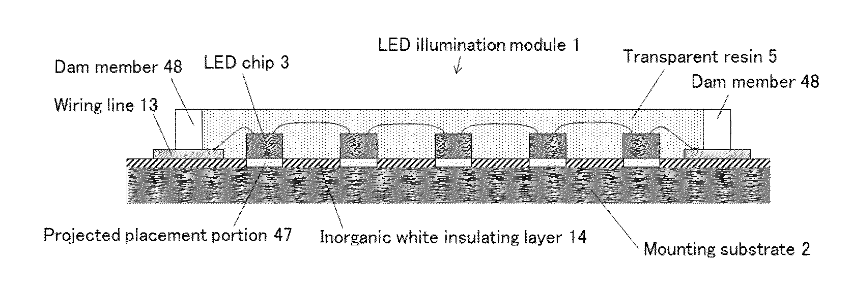
[0101]FIG. 1 is a side sectional view of an LED illumination module 1 according to a first configuration example of the present invention, and FIG. 2 is a plan view of the LED illumination module 1 according to the first configuration example of the present invention. The LED illumination module 1 according to the first configuration example includes, as main components, LED chips 3, and a mounting substrate 2 on which wiring lines 13, an inorganic white insulating layer 14, and projected placement portions 47 are formed.

[0102]The LED chips 3 are each, e.g., InGaN-based blue LED bare chip. Many LED chips 3 are arranged within a reflection region 49 in an array of n rows×m columns (e.g., 5 rows×5 columns), and are mounted by the so-called COB (Chip On Board) mounting. Each LED chip 3 is connected to the wiring line 13 or another adjacent LED chip 3 through, e.g., a thin gold wire by wire bonding. A rear surface (lower surface) of the LED chip 3 is fixed to the projected placement por...

second configuration example

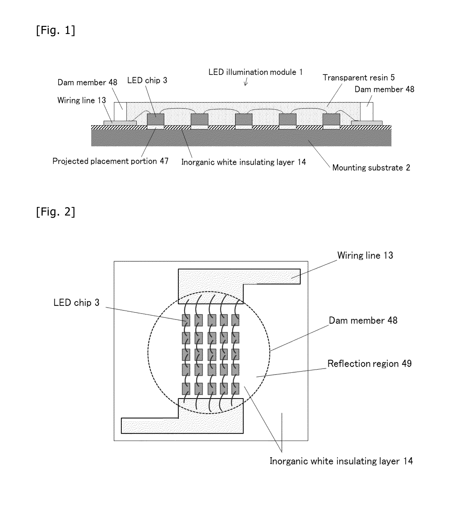
[0128]FIG. 4 is a side sectional view of an LED illumination module according to a second configuration example.

[0129]The LED illumination module 1 according to the second configuration example is similar to the module according to the first configuration example in that a plurality of LED chips 3 is COB-mounted, but is different in including a metal thin film layer 50 that is disposed on an upper surface of the mounting substrate 2.

[0130]In this configuration example, the metal thin film layer 50 made of, e.g., silver, chromium, nickel or aluminum is formed on the upper surface of the mounting substrate 2 by plating, vapor deposition, or painting. The thickness of the inorganic white insulating layer 14 can be reduced in consideration of the thickness of the metal thin film layer 50, whereby the heat radiation effect can be increased correspondingly. Moreover, the provision of the metal thin film layer 50 in the reflection region contributes to reducing irregularities in the surfac...

third configuration example

[0140]FIG. 5 is a side sectional view of an LED illumination module according to a third configuration example.

[0141]The LED illumination module 1 according to the third configuration example is different from the module according to the second configuration example in that the projected placement portions 47 are not provided on the upper surface of the mounting substrate 2 and placement portions 16 are formed instead.

[0142]In this configuration example, the metal thin film layer 50 made of, e.g., silver, chromium, nickel or aluminum is formed on the upper surface of the mounting substrate 2 by plating, vapor deposition, or painting. Then, the placement portions 16 are formed as recesses where the metal thin film layer 50 is exposed. As a result, the reflection effect and the heat dissipation effect are realized.

[0143]According to this configuration example, the reflection effect can be obtained with the exposed metal thin film layer 50 even when an area of the placement portion 16 ...


PUM


Abstract

An LED illumination module in which LED bare chips are mounted on a mounting substrate at a high density, the module comprising many LED bare chips having the same specifications, the mounting substrate at least a surface of which is metal, and a reflection region in which the LED bare chips are sealed off with resin, wherein a surface of the reflection region of the mounting substrate is covered with an inorganic white insulating layer that functions as a reflection member, a unit LED chip group including a plurality of LED bare chips connected in series is disposed plural, the plural unit LED chip groups being connected in parallel, overall light flux is 10,000 lumens or more, and a mounting area density of the LED bare chips in the reflection region is 15 mm2 / cm2 or more. An LED illumination apparatus including the LED illumination module is also provided.

Description

TECHNICAL FIELD[0001]The present invention relates to an LED illumination module and an LED illumination apparatus of a COB (Chip On Board) structure, and more particularly to an LED illumination module and an LED illumination apparatus, which emits a great amount of light at overall light flux of, e.g., 30,000 to 150,000 lumens (Inn).BACKGROUND ART[0002]Recently, many illumination appliances have been proposed in which LED (Light Emitting Diodes) are employed as light emitting units. As LED mounting methods, there are known COB mounting and package mounting. The COB mounting is practiced, for example, by mounting a semiconductor element to a flat-plate substrate on a surface of which a pattern of lead electrodes is formed using a metal film, electrically connecting the semiconductor element to the lead electrodes, and sealing the semiconductor element with resin.[0003]An LED light emitting device of COB structure is manufactured by electrically connecting an LED element, mounted on...

Claims


Application Information

Patent Timeline
Patent Type & Authority Applications(United States)
IPC IPC(8): H01L33/62F21V23/02H01L27/15H01L25/075H01L33/60F21V29/70F21V7/00
CPCH01L33/62F21V29/70F21V23/023H01L27/156H01L25/0753H01L33/60F21V7/0066H01L33/641H01L2224/48091H01L2224/48137H01L2224/45139H01L2224/45144H05K1/0274H05K2201/2054H05K2201/10106H01L2924/00014H01L2924/00H01L33/642H01L33/644H01L2924/181H01L2924/00011H01L2924/00012H01L2924/01049F21S2/005H01L33/52
Inventor ISHIHARA, MASAMICHIOYAMA, KENSHUMURAKAMI, SHOJIONOSAKA, HITONOBUSHIMA, MASATO
Owner SHIKOKU INSTR
Why Eureka
Try Eureka