Imaging element, electronic device, and information processing device

a technology of electronic devices and elements, applied in thermoelectric devices, instruments, material analysis, etc., can solve the problems of increasing the difficulty of development, increasing the level of difficulty of development, and increasing the development cost and manufacturing cost, and achieve the effect of more photoelectric conversion outputs

Active Publication Date: 2015-06-18
AMKOR TECH SINGAPORE HLDG PTE LTD +1
View PDF2 Cites 84 Cited by
  • Summary
  • Abstract
  • Description
  • Claims
  • Application Information

AI Technical Summary

Benefits of technology

[0033]According to the present disclosure, incident light is photoelectrically converted. Particularly, a wider variety of photoelectric conversion outputs are more easily provided.

Problems solved by technology

In this case, development cost and manufacturing cost considerably increase depending on situations.
In addition, development of a suitable resist is also demanded, and thus the level of difficult development may further increase.

Method used


Image

  • Imaging element, electronic device, and information processing device
  • Imaging element, electronic device, and information processing device
  • Imaging element, electronic device, and information processing device

Examples


first embodiment

1. First Embodiment

Conventional Imaging Element

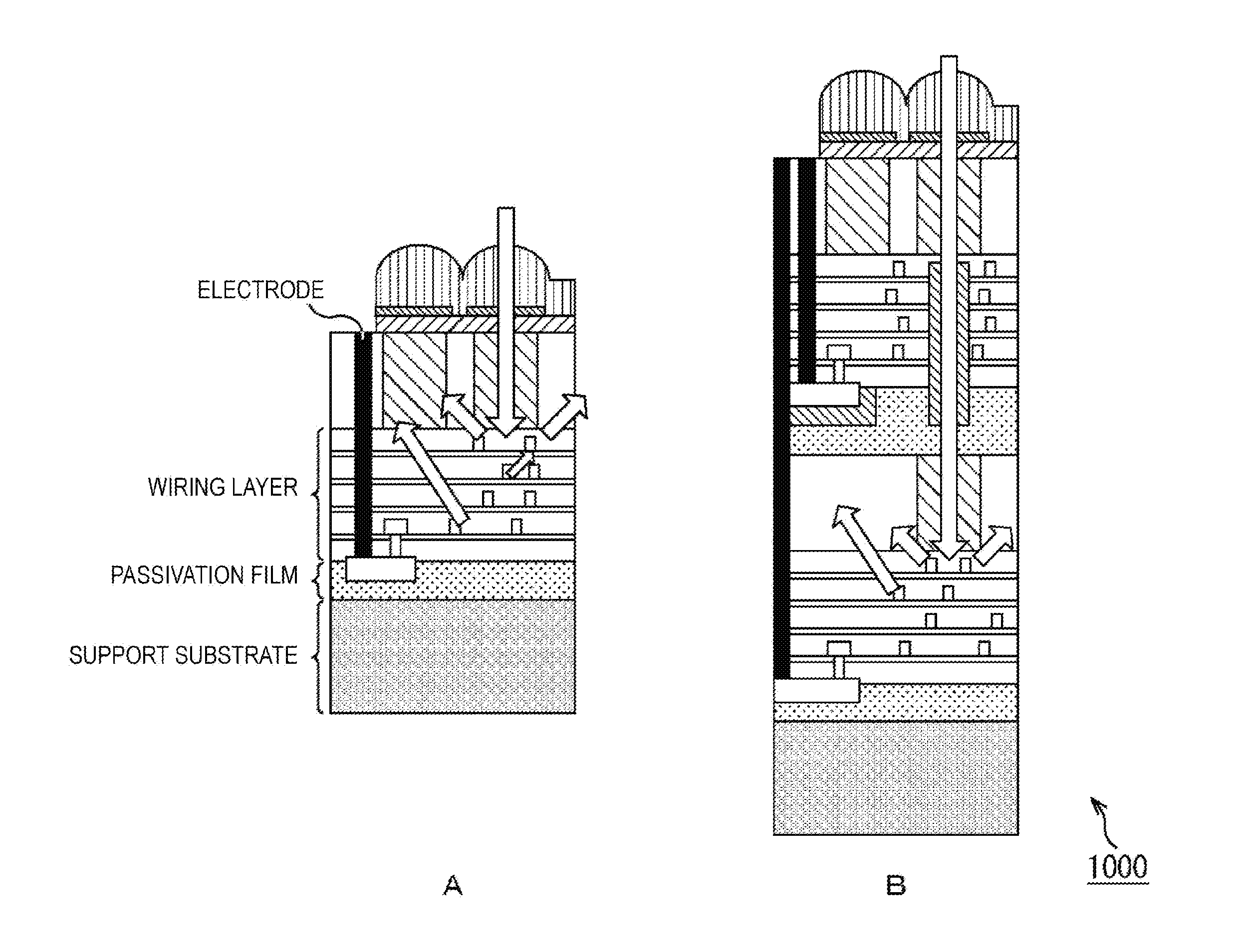
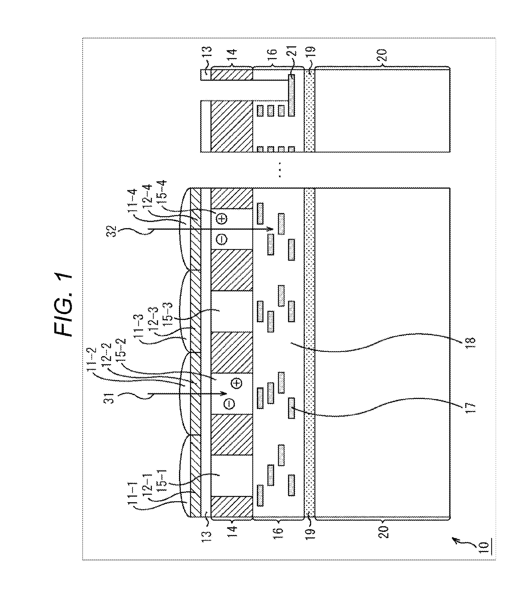
[0090]Initially, a configuration example of a conventional imaging element is discussed. FIG. 1 is a figure illustrating an example of a chief configuration of a conventional CMOS (Complementary Metal Oxide Semiconductor) image sensor. A CMOS image sensor 10 illustrated in FIG. 1 is a rear surface irradiation type image sensor including CMOS and provided with an amplifier for each unit cell.

[0091]FIG. 1 illustrates a schematic structure of the CMOS image sensor 10 in the vertical direction (lamination direction) (schematic view of cross section). As illustrated in FIG. 1, the CMOS image sensor 10 includes a condensing lens 11, a color filter 12, and a photo diode (Photo Diode) 15 for each pixel.

[0092]FIG. 1 shows four pixels as an effective pixel area of the CMOS image sensor 10. Photo diode 15-1 to photo diode 15-4 are provided in a semiconductor substrate 14 as components of the four pixels. The photo diodes 15-1 to 15-4 are collectiv...

second embodiment

2. Second Embodiment

Manufacturing Device

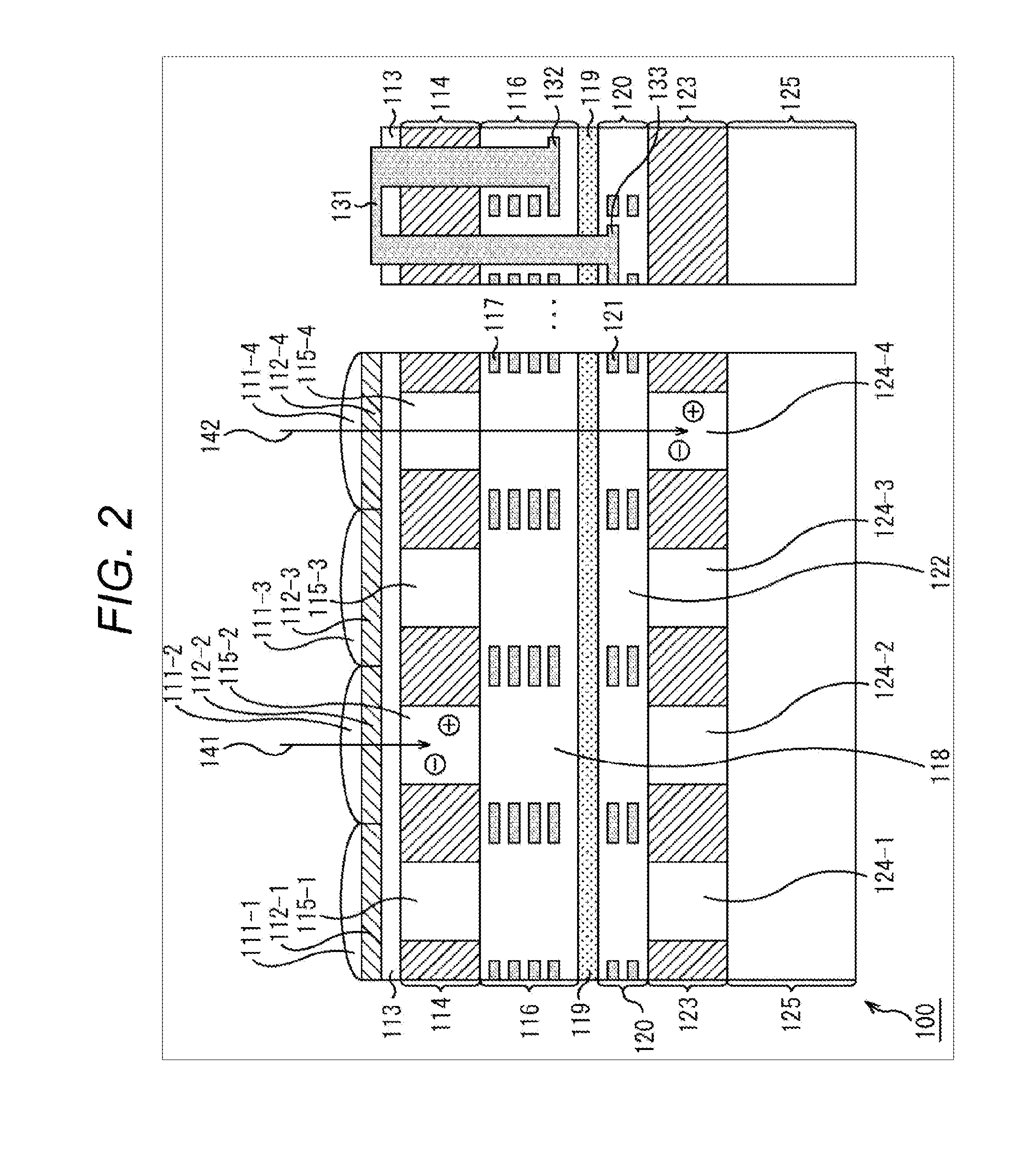
[0132]As discussed above, the CMOS image sensor 100 illustrated in FIG. 2 may be so configured that the condensing lenses 111 through the passivation film 119 constitute the rear surface irradiation type CMOS image sensor, and that the wiring layer 120 through the support substrate 125 constitute the front surface irradiation type CMOS image sensor.

[0133]Assuming that the respective CMOS image sensors are independent from each other, the CMOS image sensor 100 may be manufactured by separately producing the rear surface irradiation type CMOS image sensor and the front surface irradiation type CMOS image sensor, overlapping the front surface irradiation type CMOS image sensor on the front surface side of the produced rear surface irradiation type CMOS image sensor, and connecting both the CMOS image sensors via the TSV 131.

[0134]FIG. 3 is a block diagram illustrating an example of a chief configuration of a manufacturing device to which the pres...

third embodiment

3. Third Embodiment

Imaging Element

[0150]The CMOS image sensor 100 may have arbitrary configurations as long as a large amount of light having passed through the photo diodes 115 travels through the wiring layer 116 and the wiring layer 120 (between the respective wires of the wiring layers 116 and 120) and reach the photo diodes 124. In other words, the positions of the respective wires 117 of the wiring layer 116 and the positions of the respective wires 121 of the wiring layer 120 are arbitrarily determined as long as the optical path of incident light is secured from the diodes 115 to the photo diodes 124. For example, the wires 117 and the wires 121 may be positioned below the photo diodes 115 or above the photo diodes 124.

[0151]In addition, waveguides may be formed in the wiring layer 116, for example. FIG. 5 is a figure illustrating a configuration example of the CMOS image sensor 100 thus constructed. According to the example illustrated in FIG. 5, a waveguide 251-1 is formed...


PUM


Abstract

The present disclosure relates to an imaging element, an electronic device, and an information processing device capable of more easily providing a wider variety of photoelectric conversion outputs.
An imaging element of the present disclosure includes: a photoelectric conversion element layer containing a photoelectric conversion element that photoelectrically converts incident light; a wiring layer formed in the photoelectric conversion element layer on the side opposite to a light entering plane of the incident light, and containing a wire for reading charges from the photoelectric conversion element; and a support substrate laminated on the photoelectric conversion element layer and the wiring layer, and containing another photoelectric conversion element. The present disclosure is applicable to an imaging element, an electronic device, and an information processing device.

Description

TECHNICAL FIELD[0001]The present disclosure relates to an imaging element, an electronic device, and an information processing device, and more particularly to an imaging element, an electronic device, and an information processing device capable of more easily providing a wider variety of photoelectric conversion outputs.BACKGROUND ART[0002]The penetration length of Infrared light for silicon (Si) is long. Thus, in manufacturing a supersensitive sensor which utilizes near infrared light, a long optical length needs to be formed within silicon. Moreover, photoelectric conversion occurs at a deep position from the silicon surface corresponding to light entrance plane; therefore, a potential for storing electrons needs to be formed at a deep position.[0003]For forming a potential at a deep position, ultra-high energy ion-implantation (ion implantation) is needed according to conventional methods. In this case, development cost and manufacturing cost considerably increase depending on ...

Claims


Application Information

Patent Timeline
Patent Type & Authority Applications(United States)
IPC IPC(8): H01L27/30
CPCH01L27/307H01L27/14621H01L27/14625H01L27/14649H01L27/14645H01L27/14636H01L27/14629H01L27/1464H01L2224/48091H01L27/14605H01L27/1461H01L27/14623H01L27/14627H01L27/14647H04N23/12H10K39/32H01L2924/00014H01L25/0657
Inventor OOKI, SUSUMUNAKATA, MASASHI
Owner AMKOR TECH SINGAPORE HLDG PTE LTD
Why Eureka
Try Eureka