Method of removing oxide from substrate and method of manufacturing semiconductor device using the same

a technology of oxide removal and substrate, which is applied in the direction of semiconductor devices, solid-state devices, transistors, etc., can solve the problems of device size decline, electron tunneling that leads to gate leakage current, and non-negligible phenomena

Active Publication Date: 2015-07-09
IND ACADEMIC CORP FOUND YONSEI UNIV
View PDF1 Cites 6 Cited by
  • Summary
  • Abstract
  • Description
  • Claims
  • Application Information

AI Technical Summary

Benefits of technology

The present invention provides a method for making a semiconductor device with a thin equivalent oxide thickness and high mobility.

Problems solved by technology

However, as the device decreases in size, non-negligible phenomena have been observed, which had never been seen in a large-scaled transistor.
Particularly, when gate oxide has a thickness of about 4 nm or less, electron tunneling that leads to gate leakage current may occur.
As a result, a gate dielectric has to have a thick thickness, however, if the gate dielectric has a thick thickness, it may be difficult to maintain sufficient capacitance for operating the device.
Due to the limitation in the reducing of the size of the device, alternative methods for operating the integrated circuit at a high rate are being required.
However, the germanium has a native oxide very unstable thermally, unlike silicon oxide (SiO2) very stable thermally, diffusion of the germanium to the oxide layer at a high temperature may not be prevented.
However, the wet cleaning method may not prevent a native oxide having a thickness of about 1 nm to about 2 nm from being formed again when next gate oxide is deposited, and thus deadly defects may occur in the device.

Method used


Image

  • Method of removing oxide from substrate and method of manufacturing semiconductor device using the same
  • Method of removing oxide from substrate and method of manufacturing semiconductor device using the same
  • Method of removing oxide from substrate and method of manufacturing semiconductor device using the same

Examples


Embodiment Construction

[0040]Advantages and features of the present invention, and implementation methods thereof will be clarified through following embodiments described with reference to the accompanying drawings. The present invention may, however, be embodied in different forms and should not be construed as limited to the embodiments set forth herein. Rather, these embodiments are provided so that this disclosure will be thorough and complete, and will fully convey the scope of the present invention to those skilled in the art. Further, the present invention is only defined by scopes of claims.

[0041]Unless otherwise defined, all terms (including technical and scientific terms) used herein have the same meaning as generally understood by those skilled in the art. Terms as defined in a commonly used dictionary should be construed as having the same meaning as in an associated technical context, and unless defined apparently in the description, the terms are not ideally or excessively construed as havi...


PUM

PropertyMeasurementUnit
Energyaaaaaaaaaa
Energyaaaaaaaaaa
Energyaaaaaaaaaa

Abstract

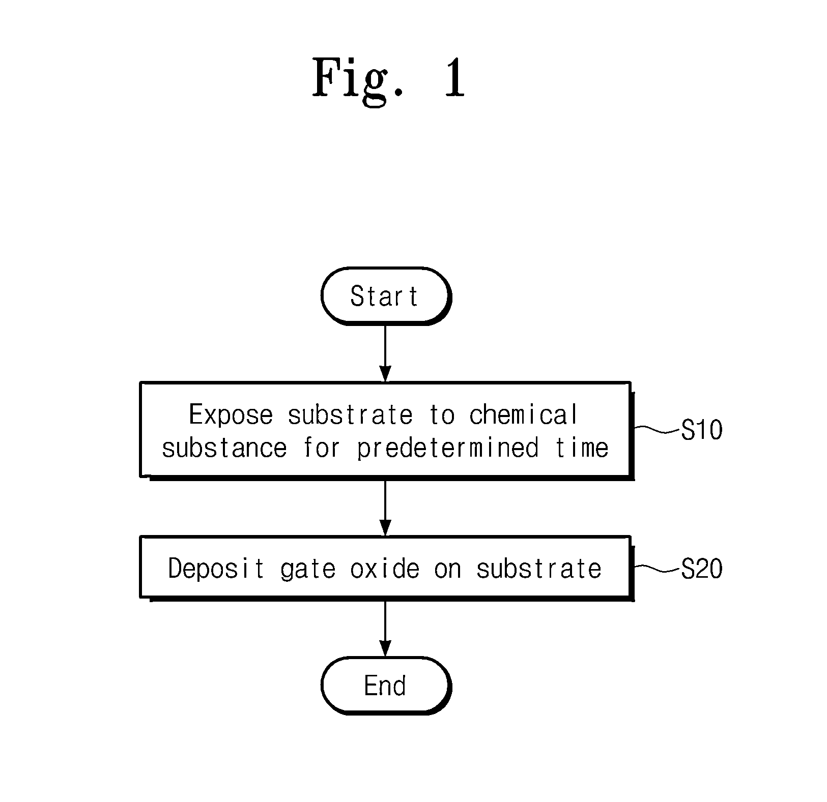
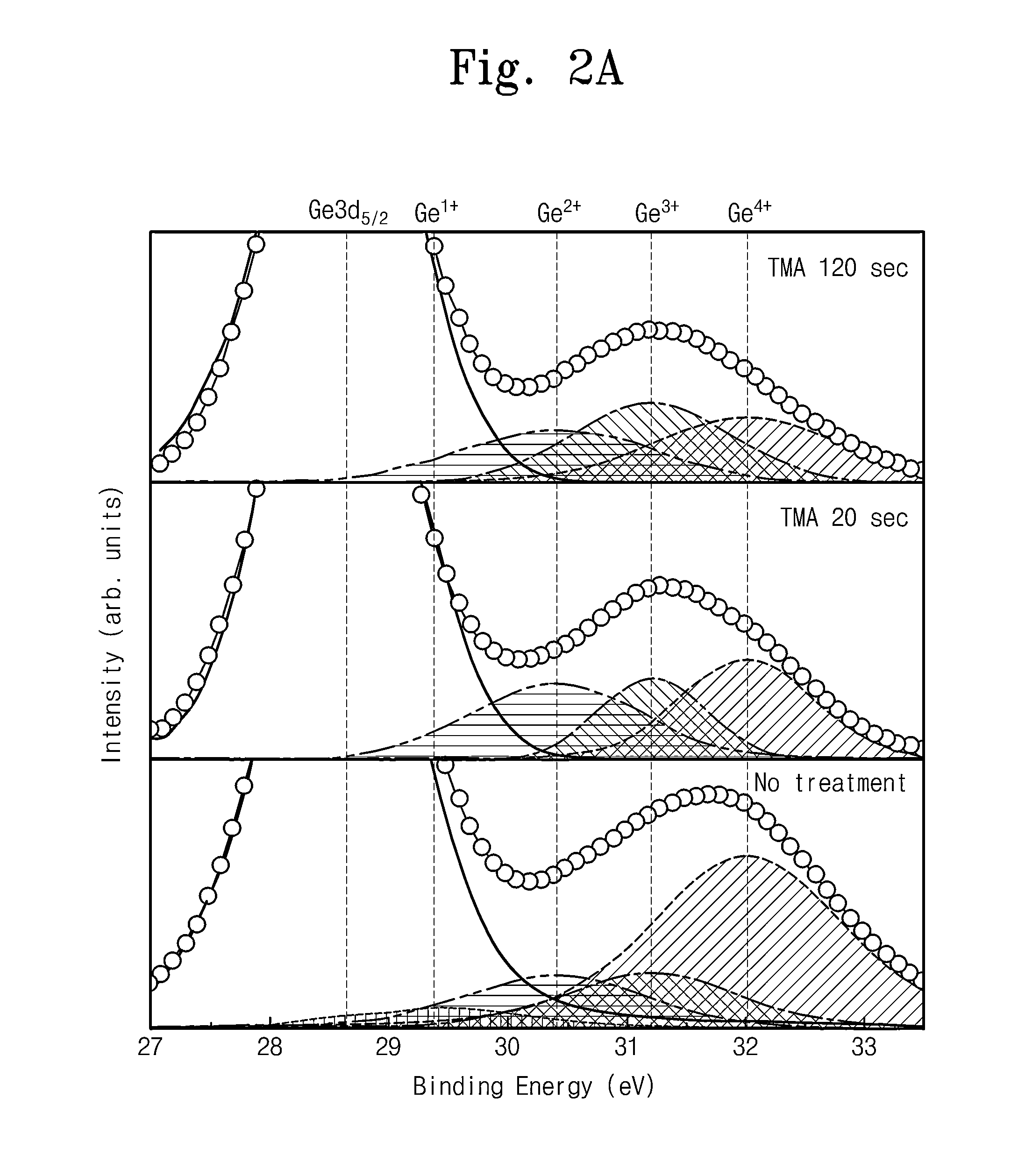
Provided is a method of removing native oxide from a substrate, the method including exposing the substrate to trimethyl aluminum (TMA) or dicyclopentadienyl magnesium (MgCp2) for a predetermined time.

Description

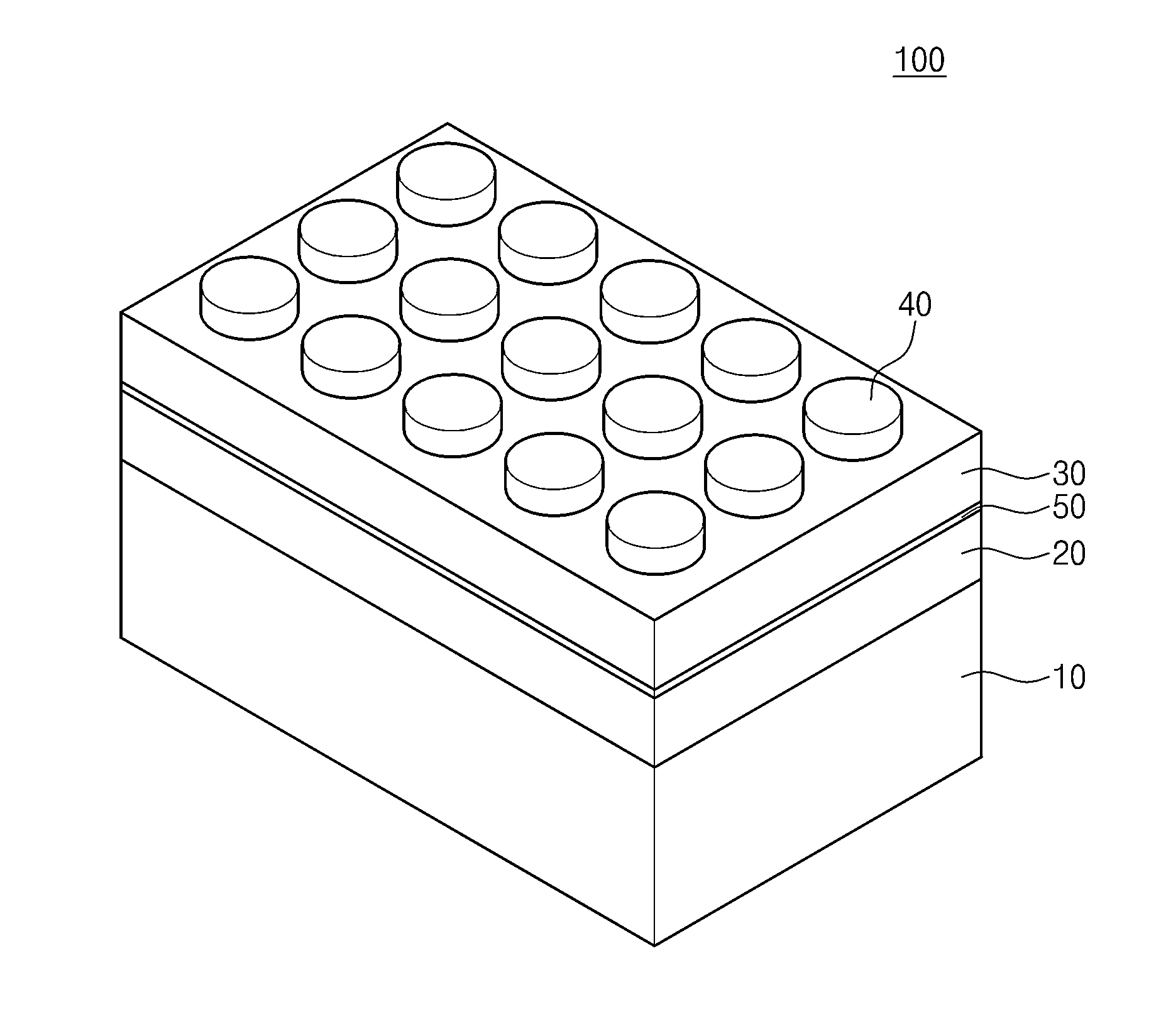
CROSS-REFERENCE TO RELATED APPLICATIONS[0001]This U.S. non-provisional patent application claims priority under 35 U.S.C. §119 of Korean Patent Application No. 10-2014-0001327, filed on Jan. 6, 2014, the entire contents of which are hereby incorporated by reference.BACKGROUND OF THE INVENTION[0002]The present invention disclosed herein relates to a method of removing an oxide from a substrate and a method of manufacturing a semiconductor device using the same.[0003]In semiconductor industries, integrated circuits have been improved in performance by simply reducing a size of a device to achieve a high response speed and low power consumption or by increasing the number of transistor to be integrated to one circuit. However, as the device decreases in size, non-negligible phenomena have been observed, which had never been seen in a large-scaled transistor. Particularly, when gate oxide has a thickness of about 4 nm or less, electron tunneling that leads to gate leakage current may oc...

Claims


Application Information

Patent Timeline
IPC IPC(8): H01L21/02H01L29/94H01L29/16H01L29/66
CPCH01L21/02043H01L21/02301H01L29/16H01L29/94H01L29/66181H01L21/02181H01L21/0228H01L21/02321H01L21/02337H01L21/02362
Inventor KIM, HYUNGJUNOH, IL-KWON
Owner IND ACADEMIC CORP FOUND YONSEI UNIV
Why Eureka
Try Eureka