

Silicon carbide semiconductor device having junction barrier schottky diode
a technology of silicon carbide and semiconductor devices, applied in the direction of semiconductor devices, basic electric elements, electrical equipment, etc., can solve problems such as affecting device yield, and achieve the effect of improving device yield
- Summary
- Abstract
- Description
- Claims
- Application Information
AI Technical Summary
Benefits of technology
Problems solved by technology
Method used
Image

Examples
first embodiment
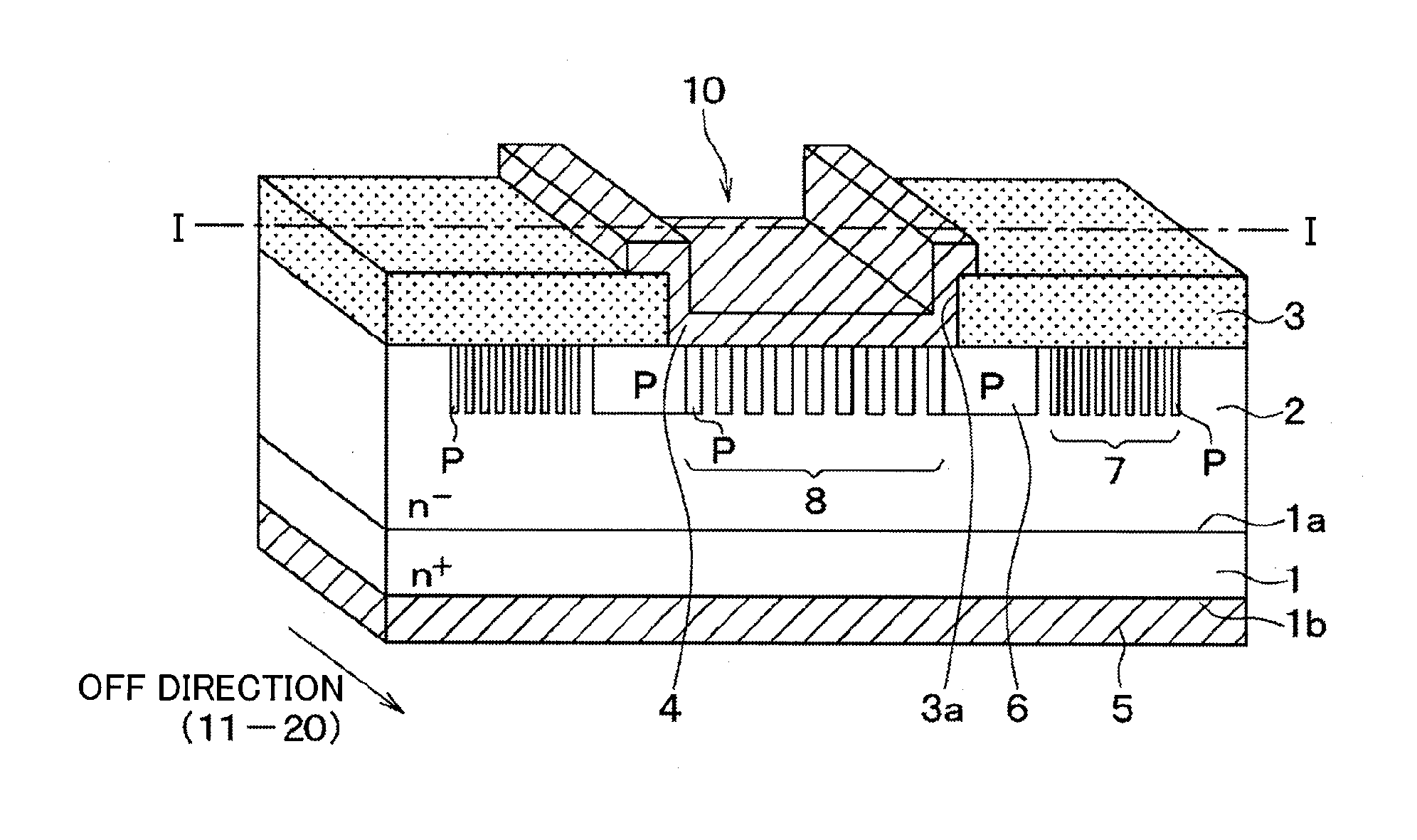
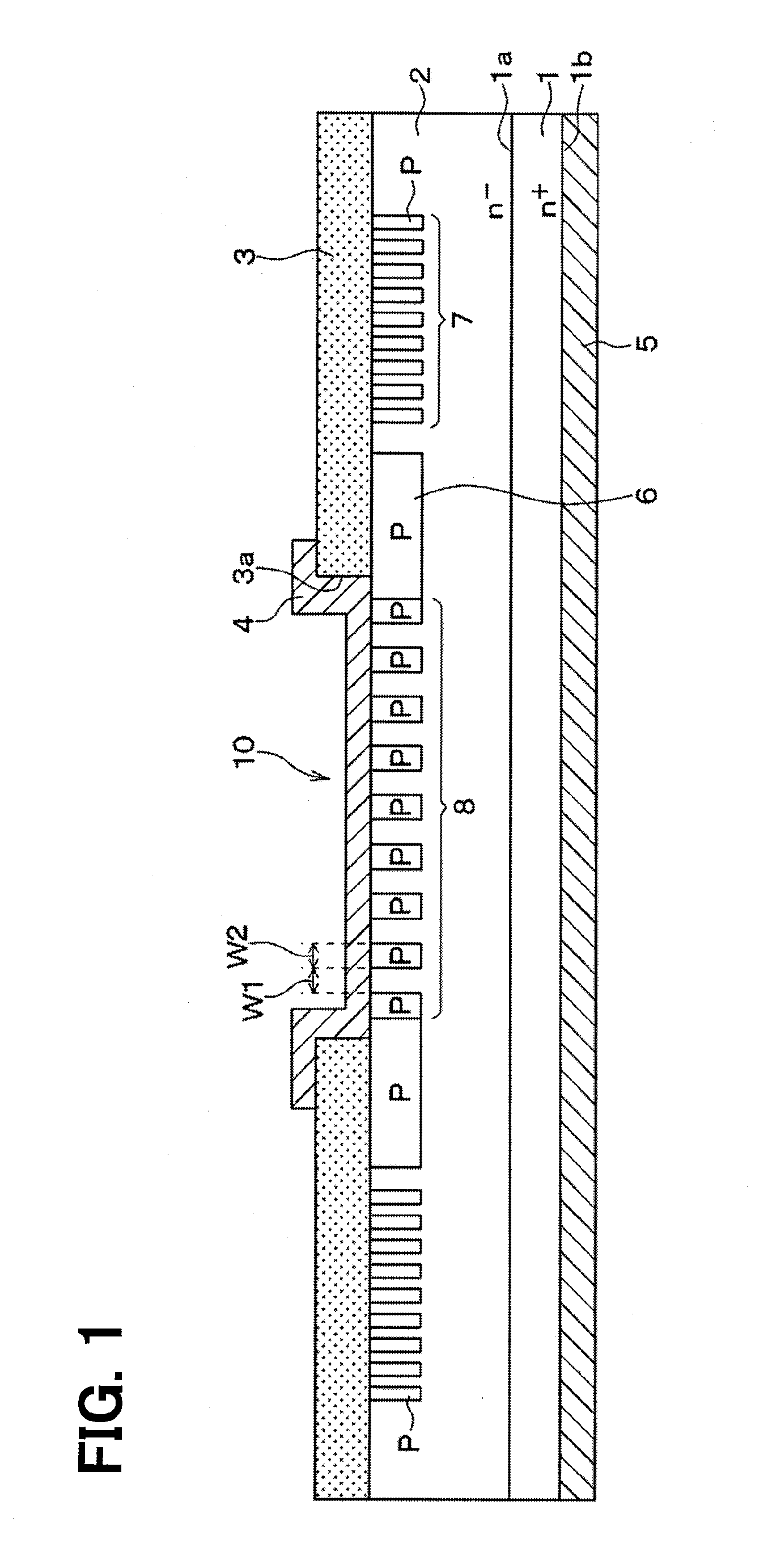
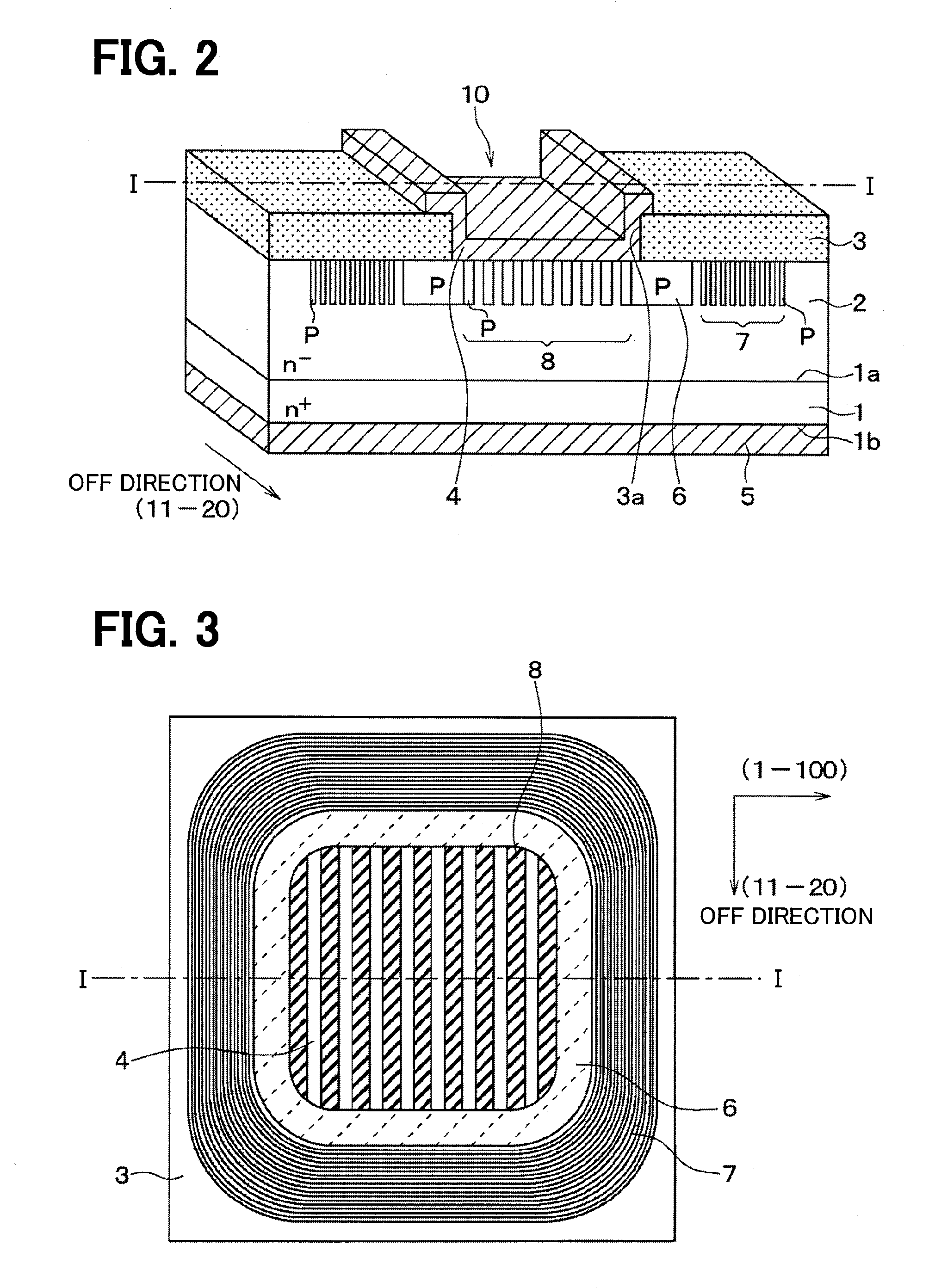
[0044]A first embodiment of the present disclosure will be described. First, a structure of an SiC semiconductor device manufactured by a method for manufacturing the SiC semiconductor device according to the present embodiment will be described with reference to FIGS. 1 to 3. FIG. 1 corresponds to a cross-sectional view taken along a line I-I in FIGS. 2 and 3. Also, although FIG. 3 is not a cross-sectional view, FIG. 3 is partially hatched for clarifying the figure.
[0045]As illustrated in FIGS. 1 and 2, the SiC semiconductor device is formed of an n+ type substrate 1 made of SiC which is, for example, about 2×10¹⁸ to 1×1021 cm−3 in impurity concentration. When it is assumed that an upper surface of the n+ type substrate 1 is a main front surface 1a, and a lower surface that is an opposite surface of the main front surface 1a is a rear surface 1b, an n− type epitaxial layer (drift layer) 2 made of SiC that is lower in dopant concentration than the substrate 1 is stacked on the main ...
second embodiment
[0061]A second embodiment of the present disclosure will be described. In the present embodiment, the off direction, the longitudinal direction of the p type layers 8, and the method for manufacturing the SiC semiconductor device are changed as compared with the first embodiment, and because the other configurations are identical with those in the first embodiment, only portions different from those in the first embodiment will be described.
[0062]As illustrated in FIG. 6, in the present embodiment, an SiC substrate having an off angle where an off direction to a (0001) plane is a (1-100) direction is used as the n+ type substrate 1. Also, the n− type epitaxial layer 2 formed on the n+ type substrate 1 is crystalline with the (1-100) direction as the off direction. Then, the p type layers 8 having longitudinal directions in the same direction as the (1-100) direction which is the off direction is formed on the n− type epitaxial layer 2 configured as described above.
[0063]Subsequently...
third embodiment
[0067]A third embodiment of the present disclosure will be described. In the present embodiment, a relationship between the off direction and the longitudinal directions of the p type layers 8, and the widths W2 of the p type layers 8 are changed as compared with the first embodiment, and because the other configurations are identical with those in the first embodiment, only portions different from those in the first embodiment will be described.
[0068]As illustrated in FIG. 8, in the present embodiment, an SiC substrate having an off angle where an off direction to a (0001) plane is a (1-100) direction is used as the n+ type substrate 1. Also, the n− type epitaxial layer 2 formed on the n+ type substrate 1 is crystalline with the (1-100) direction as the off direction. Then, the p type layers 8 having longitudinal directions in a direction perpendicular. to the (1-100) direction which is the off direction is formed on the n− type epitaxial layer 2 described above. The widths W2 of t...
PUM
 Abstract
Description
Claims
Application Information