Semiconductor device and electronic appliance

a technology of semiconductor devices and electronic appliances, applied in semiconductor devices, radiation controlled devices, electrical devices, etc., can solve the problems of excessive increase of the interface state of the semiconductor substrate, and increase of the amount of hydrogen supplied to the fine transistor in the peripheral circuit portion, so as to achieve the effect of maintaining the reliability of the fine transistor and improving the signal output characteristi

Active Publication Date: 2015-08-06
SONY CORP
View PDF9 Cites 32 Cited by
  • Summary
  • Abstract
  • Description
  • Claims
  • Application Information

AI Technical Summary

Benefits of technology

[0032]According to the present technique, in the device formed by stacking the semiconductor substrates, the reliability of the fine transistor can be maintained while the signal output characteristic is improved.

Problems solved by technology

One cause of the dark current is the increase of the interface state of the semiconductor substrate due to the plasma damage from UV irradiation or charge-up in the plasma treatment (CVD or dry etching) in the process of manufacturing the solid-state imaging element.
In the conventional structure, however, hydrogen is supplied to the entire semiconductor substrate including a pixel portion and a peripheral circuit portion; therefore, if the amount of supplying hydrogen to the pixel portion is secured, the amount of supplying hydrogen to the fine transistor in the peripheral circuit portion becomes excessive, in which case a problem occurs in that hydrogen is in excess on the semiconductor substrate surface side to deteriorate NBTI (Negative Bias Temperature Instability).

Method used


Image

  • Semiconductor device and electronic appliance
  • Semiconductor device and electronic appliance
  • Semiconductor device and electronic appliance

Examples


Embodiment Construction

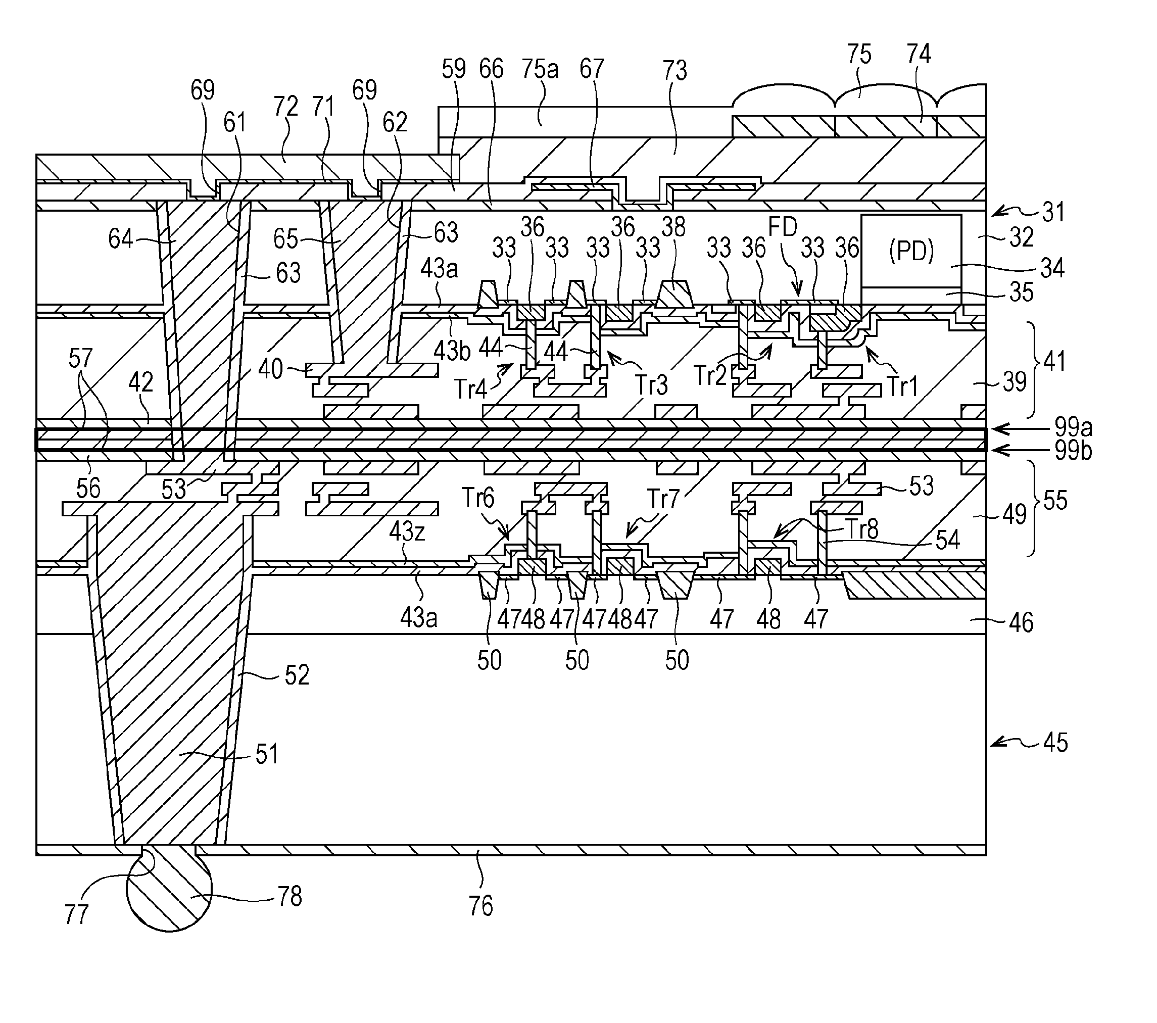
[0055]An embodiment of the technique disclosed herein is described hereinafter with reference to drawings.

[0056]First, the problem of the conventional technique is described.

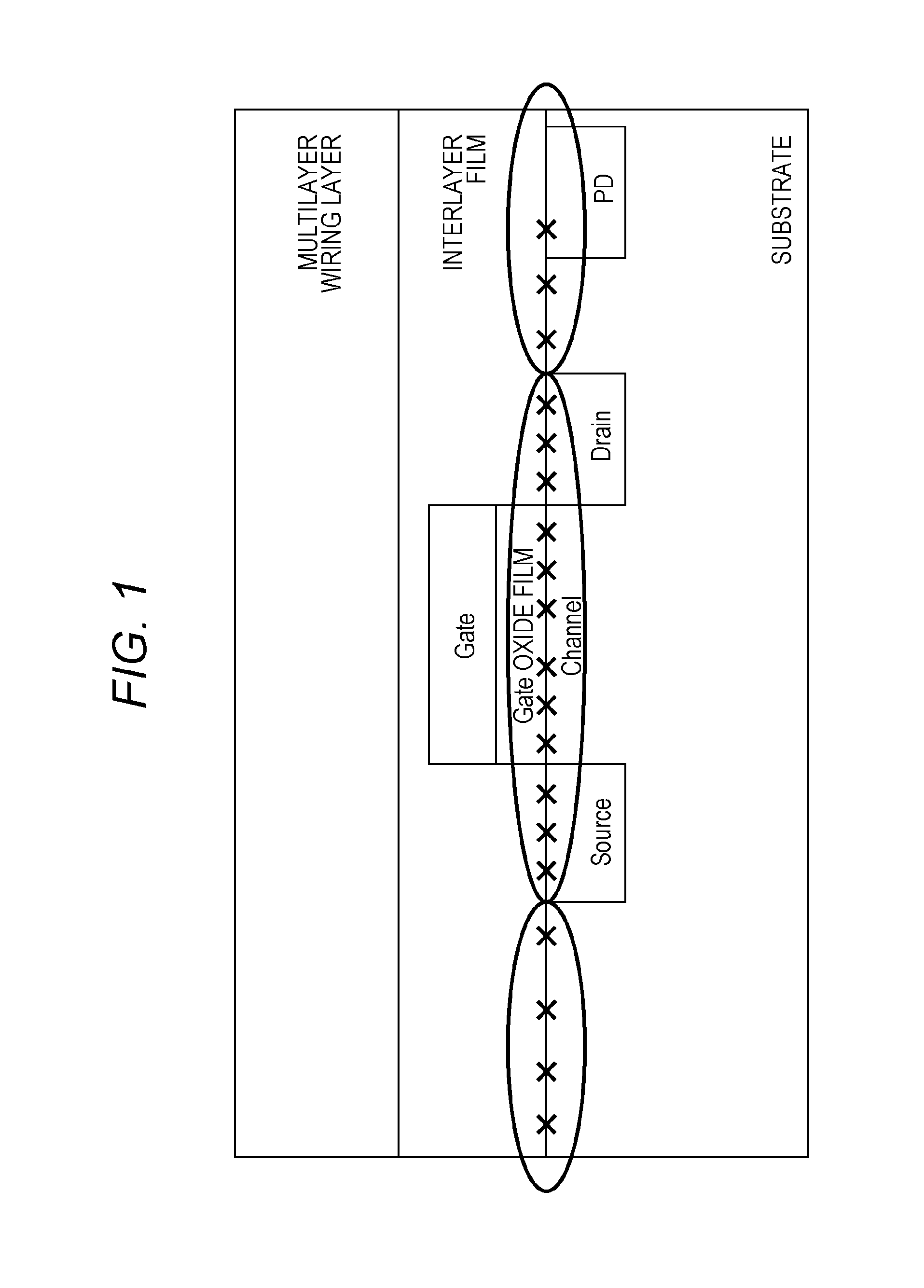
[0057]For example, in the case of forming a MOSFET, a metal electrode is connected to a source and a drain on a semiconductor substrate (semiconductor wafer) generally formed of silicon (Si).

[0058]Here, the surface of silicon (Si) is oxidized into a silicon dioxide (SiO2) film. Note that the SiO2 film is also referred to as a gate oxide film.

[0059]At the interface between Si and SiO2, the number of bonds of the atoms does not coincide perfectly; thus, uncoupled bonds of Si or oxygen (dangling bonds) remain. In this portion, electrons or holes in Si are easily captured.

[0060]It has been known that the dangling bonds at the interface between different substances, which serve to capture electrons or holes, affect the semiconductor element characteristic called the interface state.

[0061]If the interface state is pre...


PUM


Abstract

The present technique relates to a semiconductor device and an electronic appliance in which the reliability of the fine transistor can be maintained while the signal output characteristic is improved in a device formed by stacking semiconductor substrates.
The semiconductor device includes a first semiconductor substrate, a second semiconductor substrate providing a function different from a function provided by the first semiconductor substrate, and a diffusion prevention film that prevents diffusion of a dangling bond terminating atom used for reducing the interface state of the first semiconductor substrate and the second semiconductor substrate, wherein at least two semiconductor substrates are stacked and the semiconductor substrates are electrically connected to each other, and the first semiconductor substrate and the second semiconductor substrate are stacked with the diffusion prevention film inserted between an interface of the first semiconductor substrate and an interface of the second semiconductor substrate.

Description

TECHNICAL FIELD[0001]The present technique relates to a semiconductor device and an electronic appliance, and particularly to a semiconductor device and an electronic appliance, which are formed by stacking semiconductor substrates and in which the reliability of fine transistors can be maintained while the signal output characteristic is improved.BACKGROUND ART[0002]In regard to a conventional solid-state imaging element, it is important to reduce the dark current on a surface of a semiconductor substrate, which causes the deterioration in image quality, and to improve the characteristic of the flicker noise or random telegraph noise of a pixel transistor in a CCD or CMOS image sensor.[0003]One cause of the dark current is the increase of the interface state of the semiconductor substrate due to the plasma damage from UV irradiation or charge-up in the plasma treatment (CVD or dry etching) in the process of manufacturing the solid-state imaging element.[0004]For improving the pixel...

Claims


Application Information

Patent Timeline
Patent Type & Authority Applications(United States)
IPC IPC(8): H01L27/146
CPCH01L27/14634H01L27/1462H01L27/1469H01L27/1464H01L27/14636H01L2224/11H01L2924/13091H01L2924/00H01L25/167
Inventor BABA, KOICHIKUBODERA, TAKASHIMIYAZAKI, TOSHIHIKOAMMO, HIROAKI
Owner SONY CORP
Why Eureka
Try Eureka