Light-emitting device

a technology of light-emitting devices and substrates, which is applied in the direction of solid-state devices, semiconductor devices, thermoelectric devices, etc., can solve the problems of cracks, cracks, and cracks in the end portion of the layer to be separated in the separation and dividing steps, so as to reduce the risk of cracks , the effect of high reliability

Active Publication Date: 2015-09-10
SEMICON ENERGY LAB CO LTD
View PDF8 Cites 62 Cited by
  • Summary
  • Abstract
  • Description
  • Claims
  • Application Information

AI Technical Summary

Benefits of technology

[0023]According to one embodiment of the present invention, a flexible light-emitting device with fewer defects caused by a crack can be provided. Alternatively, a flexible light-emitting device with high productivity can be provided. A light-emitting device with high reliability can also be provided.
[0024]According to another embodiment of the present invention, a novel light-emitting device can be provided. Alternatively, a lightweight light-emitting device can be provid

Problems solved by technology

The stack has a thickness of several micrometers or less and is very fragile in some cases.
At this time, due to stress applied when the substrate is divided, a crack might occur in a thin film in an end portion of the substrate, particularly in the layer to be separated.
In addition, when the flexible light-emitting device that is manufactured in the aforementioned separating and dividing steps is held in

Method used


Image

  • Light-emitting device
  • Light-emitting device
  • Light-emitting device

Examples


embodiment 1

[0051]In this embodiment, an example of a structure and a manufacturing method of an image display device, which is an example of a light-emitting device of one embodiment of the present invention, will be described with reference to drawings. As an example of the image display device, an image display device (hereinafter, also referred to as display device) including an organic electroluminescence (EL) element will be described below.

[Structure Example of Display Device]

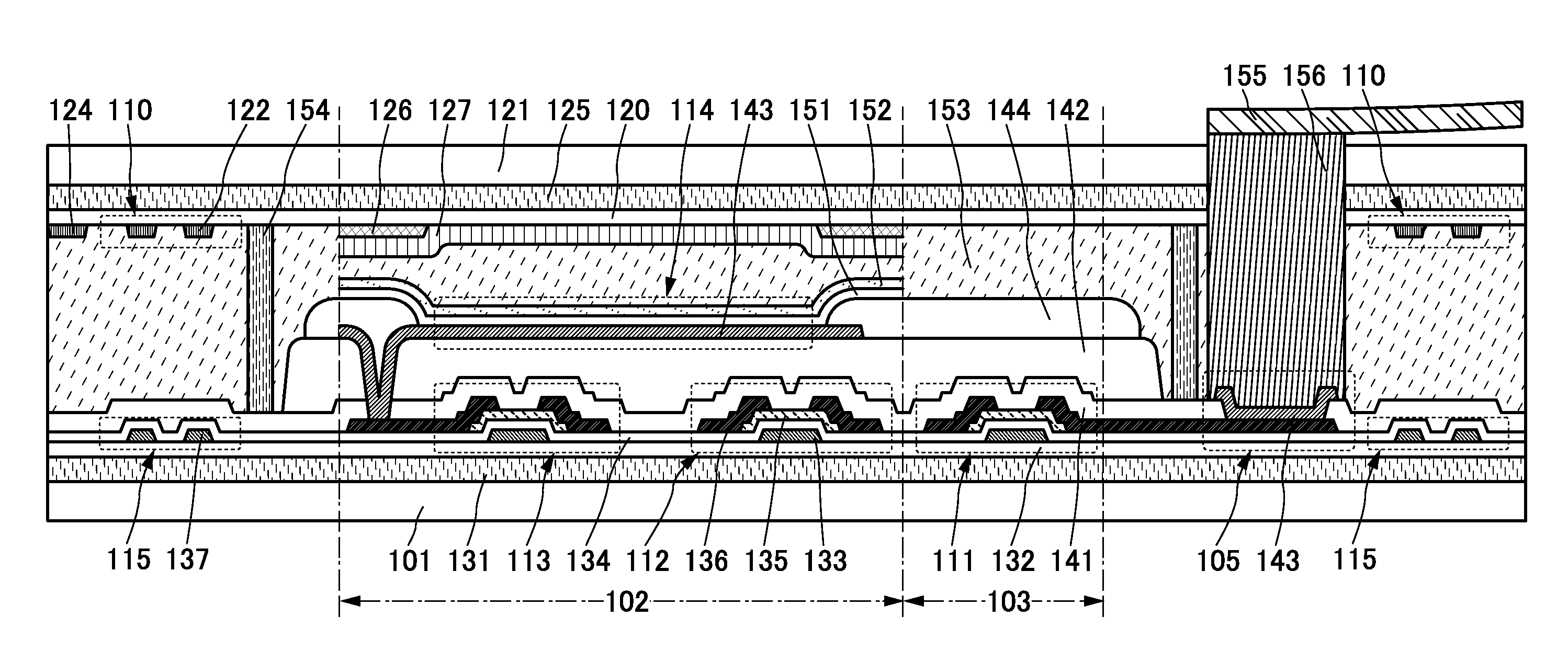
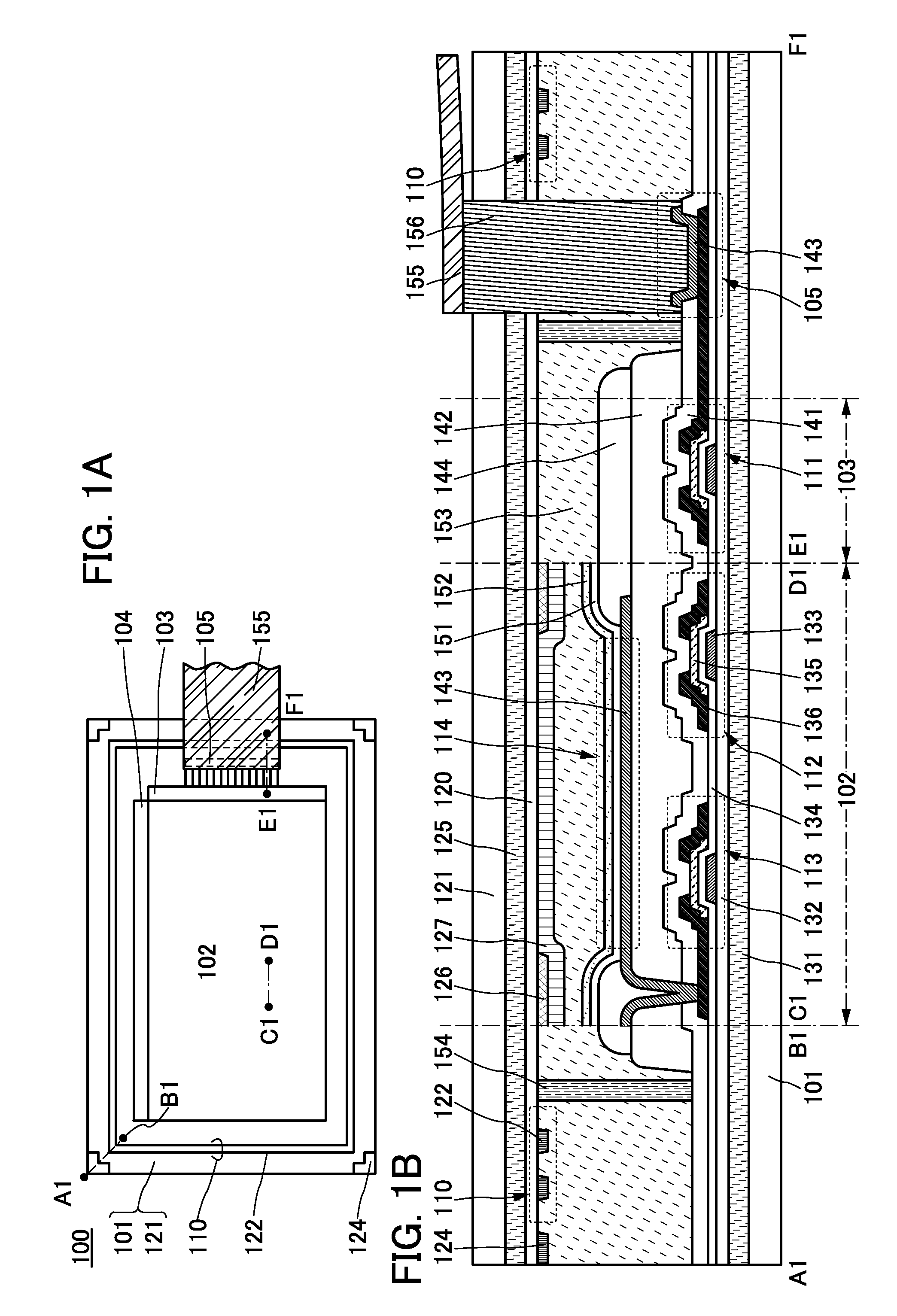
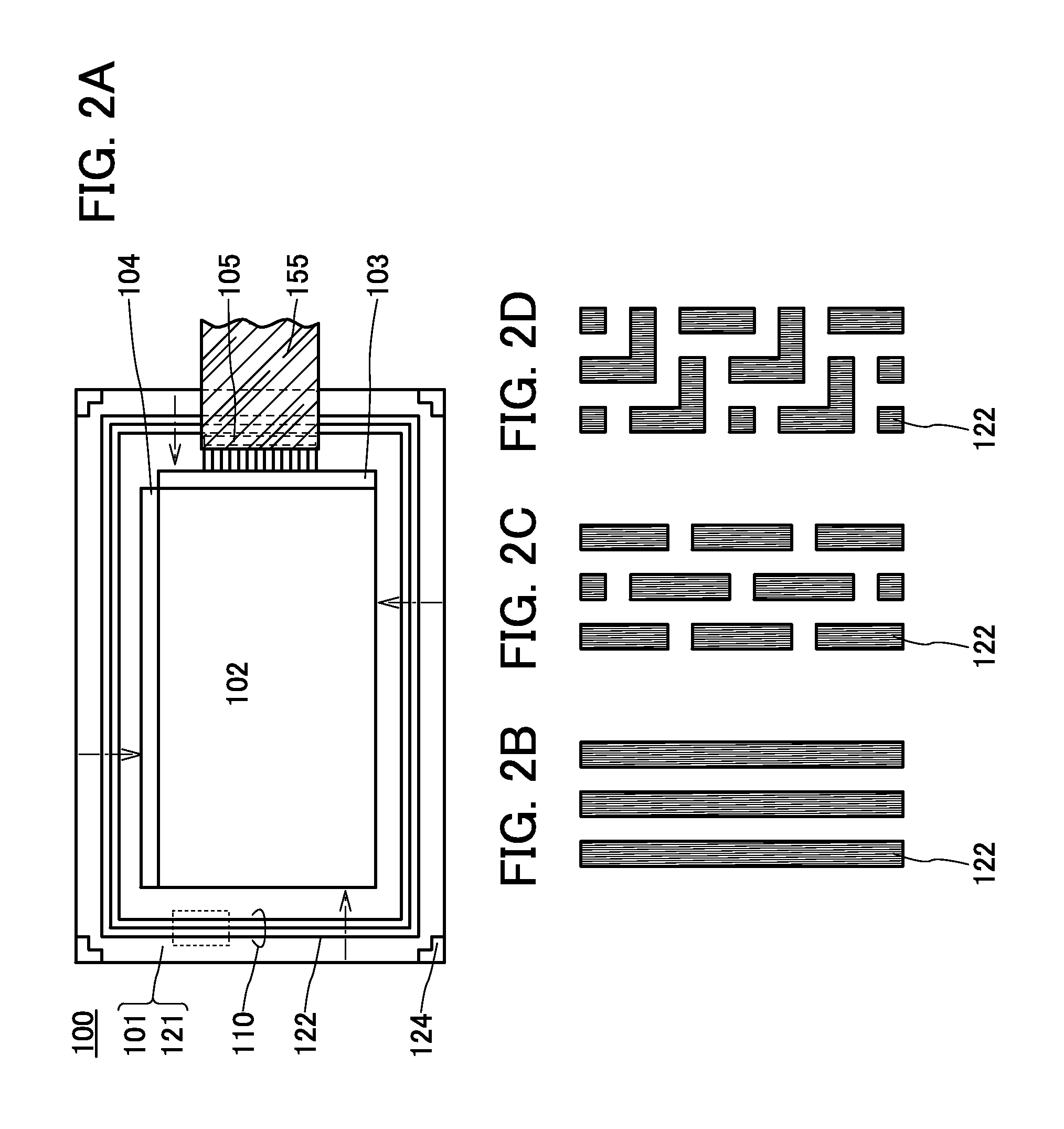
[0052]FIG. 1A is a schematic top view of a display device 100 with a top emission structure. Note that in FIG. 1A, some components are not illustrated for clarity.

[0053]FIG. 1B is a schematic cross-sectional view of FIG. 1A along line A1-B1 passing through a region including one of the four corners of the second substrate 101, along line C1-D1 passing through part of a display portion 102, and along line E1-F1 passing through a region including a signal line driver circuit 103 and an external connection terminal 105...

modification example 1

[0211]FIG. 9 is a schematic cross-sectional view of the display device 100 that includes a cover layer 123 in contact with the crack inhibiting layer 122.

[0212]In the case where the marker 124 is not formed in the display device 100, the crack inhibiting layer 122 is preferably formed using the same material as the black matrix 126 so as not to increase the number of steps.

[0213]To prevent a crack more effectively, the cover layer 123 may be formed to cover a plurality of crack inhibiting layers 122. The development of the crack can be hindered when stress is distributed unevenly in the direction where the crack develops at the interface between the buffer layer 120 and each of the crack inhibiting layers 122 and the cover layer 123. Therefore, the cover layer 123 is preferably formed using a material different from that of the crack inhibiting layers 122. The cover layer 123 can be formed of a conductive material or a resin material.

[0214]In the display device 100 illustrated in FI...

modification example 2

[0216]FIG. 10 is a schematic cross-sectional view of the display device 100 that includes a second crack inhibiting region 115 over the buffer layer 132.

[0217]In the display device 100 illustrated in FIG. 10, the second crack inhibiting region 115 including a plurality of second crack inhibiting layers 137 is provided to overlap with the crack inhibiting region 110. When the second crack inhibiting region 115 is provided to surround not only the display portion 102 but also the signal line driver circuit 103, the scan line driver circuit 104, the external connection terminal 105, and the like, a crack generated from an end portion of the second buffer layer 132 can be prevented from reaching these portions, inhibiting failure such as the malfunction of the display device 100.

[0218]Note that the second crack inhibiting layer 137 is preferably formed in contact with the second buffer layer 132 with use of a conductive material or a resin material similarly to the crack inhibiting laye...


PUM


Abstract

A flexible device with fewer defects caused by a crack is provided. A flexible device with high productivity is also provided. Furthermore, a flexible device with less display failure even in a high temperature and high humidity environment is provided. A light-emitting device includes a first flexible substrate, a second flexible substrate, a buffer layer, a first crack inhibiting layer, and a light-emitting element. A first surface of the first flexible substrate faces a second surface of the second flexible substrate. The buffer layer and the first crack inhibiting layer are provided over the first surface of the first flexible substrate. The buffer layer overlaps with the first crack inhibiting layer. The light-emitting element is provided over the second surface of the second flexible substrate.

Description

TECHNICAL FIELD[0001]One embodiment of the present invention relates to a display device, and particularly to a flexible display device capable of performing display along a curved surface. One embodiment of the present invention also relates to a light-emitting device, and particularly to a flexible light-emitting device capable of performing light emission along a curved surface.[0002]Note that one embodiment of the present invention is not limited to the above technical field. The technical field of one embodiment of the invention disclosed in this specification and the like relates to an object, a method, or a manufacturing method. In addition, one embodiment of the present invention relates to a process, a machine, manufacture, or a composition of matter. Specifically, examples of the technical field of one embodiment of the present invention disclosed in this specification include a semiconductor device, a display device, a light-emitting device, an electronic device, a method...

Claims


Application Information

Patent Timeline
IPC IPC(8): H01L51/00H01L27/32H01L51/52
CPCH01L51/0097H01L27/323H01L51/524H01L51/5253Y02E10/549H10K59/40H10K77/111H10K50/841H10K2102/311H10K50/844H10K50/865H10K50/8426H10K50/84H10K50/8423
Inventor NAKADA, MASATAKAABE, TAKAYUKISENDA, NAOYUKI
Owner SEMICON ENERGY LAB CO LTD
Why Eureka
Try Eureka