Methods for forming interconnection structures in an integrated cluster system for semicondcutor applications

a technology of semiconductor and interconnection structure, which is applied in the direction of basic electric elements, electrical equipment, electric discharge tubes, etc., can solve the problems of reducing the overall performance of the integrated circuit, reducing the accuracy of pattern transfer, and increasing the difficulty of pattern transfer for the manufacture of structures with small critical dimensions and high aspect ratios

Active Publication Date: 2015-09-17
APPLIED MATERIALS INC
View PDF10 Cites 29 Cited by
  • Summary
  • Abstract
  • Description
  • Claims
  • Application Information

AI Technical Summary

Benefits of technology

[0011]Embodiments of the present invention provide methods for forming an interconnection structure in semiconductor devices without breaking vacuum with minimum oxidation / atmosphere exposure. In one embodiment, a method for forming an interconnection structure for semiconductor devices includes supplying a barrier layer etching gas mixture into a first processing chamber having a substrate disposed therein to etch portions of a barrier layer exposed by a patterned metal layer until the underlying substrate is exposed, the first processing chamber disposed in a processing system, and forming a liner layer on the substrate covering the etched barrier layer in a second processing chamber disposed in the processing system.

Problems solved by technology

Integrated circuits have evolved into complex devices that can include millions of transistors, capacitors and resistors on a single chip.
As the geometry limits of the structures used to form semiconductor devices are pushed against technology limits, the need for accurate pattern transfer for the manufacture of structures have small critical dimensions and high aspect ratios has become increasingly difficult.
Capacitive coupling between adjacent metal interconnects may cause cross talk and / or resistance-capacitance (RC) delay which degrades the overall performance of the integrated circuit.
However, several disadvantages associated with copper damascene structure have become severe concerns as feature sizes continue to decrease.
For example, small feature size of the metal lines generally requires higher aspect ratio, which may adversely increase difficulty to fill such features to form void free metal structures.
Forming a barrier layer within high aspect features is particularly difficult.
Furthermore, as feature sizes continue to decrease, the barrier layer cannot scale, thus resulting the barrier layer in greater fraction of that particular feature.
However, after the metal etching process, the metal interconnection is often exposed to air.
Excess exposure of the metal conductive materials to air may adversely affect the nucleation capability of the metal elements to adhere to the substrate surface during a subsequently metallization process.
Furthermore, poor adhesion at the interface may also result in undesired high contact resistance, thereby resulting in undesirably poor electrical properties of the device.
In addition, poor nucleation of the metal elements in the back end interconnection may impact not only the electrical performance of the devices, but also on the integration of the conductive contact material subsequently formed thereon.
However, in some cases, inadequate control of the Q-times in the processes of forming and patterning each layer, including the metal layer and passivation protection, may adversely result in excess oxidation formed onto the metal surface, thereby in high contact resistance and poor adhesion.
Overly long exposure time of each layer in the interconnection structure to air or ambient may also undesirably create contamination sources or oxidation growth at the interface, resulting in film degradation and eventually leading to device failure.

Method used


Image

  • Methods for forming interconnection structures in an integrated cluster system for semicondcutor applications
  • Methods for forming interconnection structures in an integrated cluster system for semicondcutor applications
  • Methods for forming interconnection structures in an integrated cluster system for semicondcutor applications

Examples


Embodiment Construction

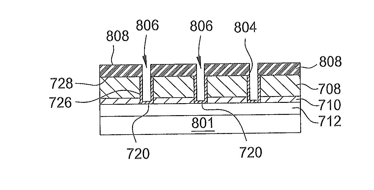
[0025]Embodiments of the present invention provide methods for forming an interconnection structure in semiconductor devices without breaking vacuum with minimum oxidation / atmosphere exposure. In one embodiment, the interconnection structure may be formed by utilizing a dry etching process to etch a metal layer and a barrier layer, and subsequently forming liner layer on the substrate without breaking vacuum. The processes for forming the interconnection structure may be all integrated and performed in a processing system, i.e., a cluster system, to deposit, form and pattern layers in a single processing system without breaking vacuum so as to reduce the likelihood of surface oxidation, contamination, thereby providing a good control of profile formation and electrical properties for semiconductor devices.

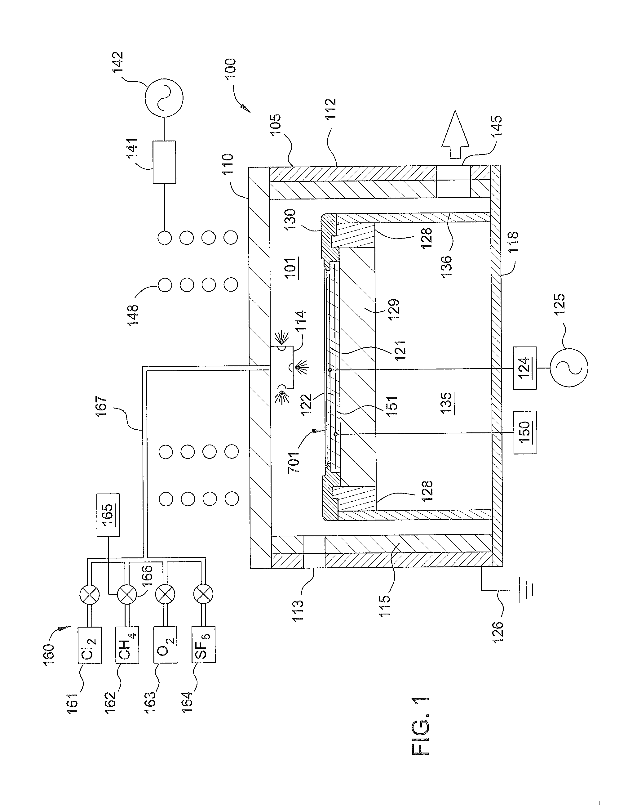
[0026]FIG. 1 is a simplified cutaway view for an exemplary etch processing chamber 100 for etching a metal layer. The exemplary etch processing chamber 100 is suitable for removing...


PUM


Abstract

Embodiments of the present invention provide methods for forming an interconnection structure in semiconductor devices without breaking vacuum with minimum oxidation/atmosphere exposure. In one embodiment, a method for forming an interconnection structure for semiconductor devices includes supplying a barrier layer etching gas mixture into a first processing chamber having a substrate disposed therein to etch portions of a barrier layer exposed by a patterned metal layer until the underlying substrate is exposed, the first processing chamber disposed in a processing system, and forming a liner layer on the substrate covering the etched barrier layer in a second processing chamber disposed in the processing system.

Description

[0001]This application claims benefit of U.S. Provisional Patent Application Ser. No. 61 / 951,386, filed Mar. 11, 2014, which is incorporated by reference in its entirety.BACKGROUND[0002]1. Field[0003]Embodiments of the present invention generally relate to methods of patterning a metal layer, and more particularly to methods of forming an interconnection structure in an integrated cluster system without breaking vacuum in semiconductor applications.[0004]2. Description of the Related Art[0005]Integrated circuits have evolved into complex devices that can include millions of transistors, capacitors and resistors on a single chip. The evolution of chip designs continually requires faster circuitry and greater circuit density. The demands for faster circuits with greater circuit densities impose corresponding demands on the materials used to fabricate such integrated circuits. In particular, as the dimensions of integrated circuit components are reduced to the sub-micron scale, it is n...

Claims


Application Information

Patent Timeline
Patent Type & Authority Applications(United States)
IPC IPC(8): H01L21/768H01L21/02H01L21/3213
CPCH01L21/76841H01L21/32136H01L21/76829H01L21/02068H01L21/02167H01L21/02071H01L21/02274H01L21/32139H01L21/67184H01L21/67207H01J37/321H01J37/32357H01J37/3244H01L21/76885H01L21/76834H01L21/7685
Inventor NAIK, MEHUL B.NEMANI, SRINIVAS D.KOSHIZAWA, TAKEHITOREN, HE
Owner APPLIED MATERIALS INC
Why Eureka
Try Eureka