Multilayer getter structures and methods for making same

a multi-layer, getter technology, applied in the direction of solid cathodes, gas-filled discharge tubes, x-ray tubes, etc., can solve the problems of low gas sorbing properties, short neg operating life, and inability to manufacture certain devices, etc., to achieve low activation and high surface area

Active Publication Date: 2008-08-19
SAES GETTERS SPA
View PDF28 Cites 16 Cited by
  • Summary
  • Abstract
  • Description
  • Claims
  • Application Information

AI Technical Summary

Benefits of technology

[0015]An embodiment of the present invention provides a multilayer arrangement of non-evaporable getter materials, including a first or under layer of non-evaporable getter material having a relatively high surface area and, upon the first layer, a relatively thin second or over layer of a non-evaporable getter alloy with low activation temperature. The layers are preferably obtained by cathodic deposition, with minimal exposure of the first layer to reactive gases occurring between the deposition of the two layers.
[0018]Advantageously, the multilayer structures of the invention provide a large effective surface area and have a low activation temperature, providing great operating and activation efficiencies. This and other advantages of the present invention will become more fully apparent when the following detailed description of the invention is read in conjunction with the accompanying drawing(s).

Problems solved by technology

In theory, complete activation of an NEG would generally be desirable, but it can be unfeasible in the manufacture of certain devices, due to restrictions on manufacturing times and / or heat sensitivity of the particular device.
Accordingly, partial activation is used for such devices, even though this results in lower gas sorbing properties and shorter NEG operating life.
For some materials, complete activation can require very high temperatures.
For an effective activation (or reactivation), however, pure metals require comparatively high temperatures, generally higher than 450° C. In miniaturized devices such as FEDs or MEMs, wherein the NEG material is quite close to functional or structural parts of the device, the activation treatment can damage these parts.
For example, in the case of FEDs, in which the NEG is generally placed at the peripheric region, heating at 400° C. can compromise the tightness of sealing between the two glass parts forming the display, which are made up of a low-melting glass paste.
Similarly, exposure to these temperatures can compromise sealings between silicon components of MEMs, which are often composed of brazing alloys such as silver-based alloys or gold-tin or gold-indium alloys.
However, the present inventors have determined that these materials, when deposited by sputtering, give rise to thin layers having extremely compact morphology and consequently a very reduced effective surface area, generally equivalent to only a few times the deposit geometrical area.
This characteristic limits considerably the deposit sorbing properties at room temperature, particularly its initial sorption rate and its capacity.
Such materials would require frequent reactivation, which may be impractical or impossible in certain applications.
Accordingly, currently known NEG deposits obtained by sputtering either have poor sorbing characteristics at room temperature (in particular, a low sorption rate) or require high activation temperatures incompatible with some applications, particularly in miniaturized devices.

Method used


Image

  • Multilayer getter structures and methods for making same
  • Multilayer getter structures and methods for making same
  • Multilayer getter structures and methods for making same

Examples


example 1

Preparation of a Multilayer Deposit Having Titanium Underlayer (3.3 μm) and ZrV2 Over Layer

[0055]This example provides an exemplary preparation of a double-layered deposit according to the invention.

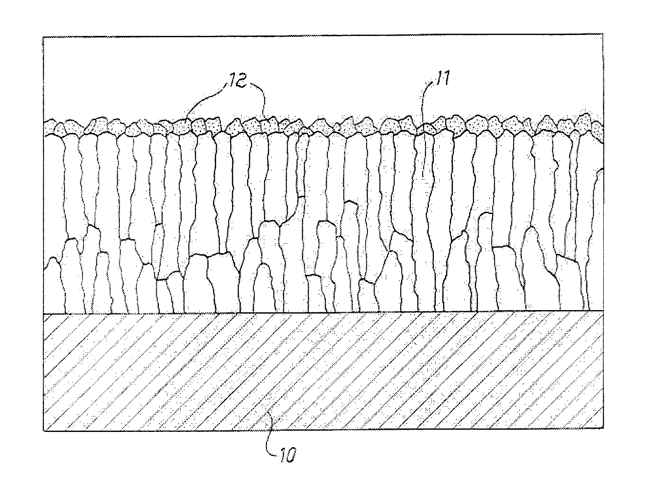
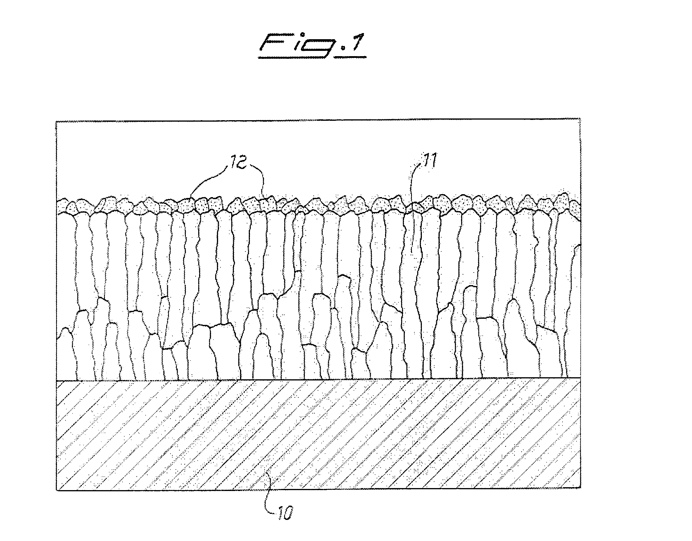
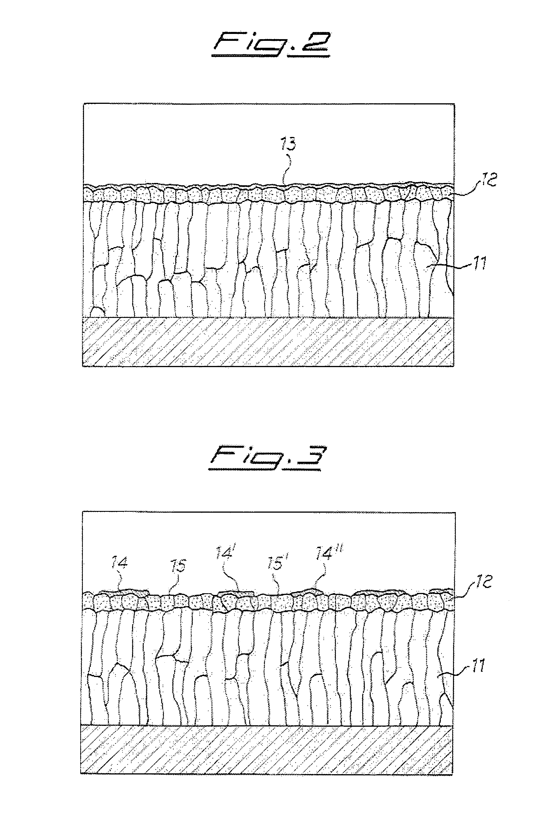
[0056]A polished monocrystalline silicon disc having a diameter of 2.5 cm was cleaned in an ultrasonic bath with an organic solvent (an alcoholic solution of n-propylbromide) and subsequently rinsed in deionized water. This support was placed into a cathodic deposition chamber that can contain up to three targets of different materials. The chamber was evacuated to a pressure of 3×10⁻⁶ Pa, then backfilled with argon to a pressure of 2 Pa. A titanium layer was first deposited, with the following operating parameters:[0057]power density on the target: 3.5 W / cm2;[0058]target-support distance: 140 mm;[0059]support temperature: 100° C.;[0060]deposition time: 80 minutes.

[0061]Subsequently a second target of a ZrV2 alloy was used, a layer of which was deposited on the titanium layer, employing ...

example 4

Preparation of a Multilayer Deposit Having Titanium Underlayer (1.6 μm) and ZrV2 Overlayer

[0068]The procedure of the Example 1 is repeated, with the exception that the titanium deposition lasts 40 minutes. The average thickness of the two layers was shown by electron microscopy to be 1.6 μm for the titanium layer and 0.2 μm for the ZrV2 alloy.

[0069]This support having a two-layer deposit was designated sample 4.

example 5

Room Temperature Gas Sorption of Monolayer and Multilayer Deposits

[0070]In this example, the gas sorbing properties at room temperature of samples 1, 2 and 3, prepared as described above, are evaluated.

[0071]The samples were mounted one at a time into a quartz bulb, which was evacuated before every test through a turbomolecular pump to a residual pressure of 1×10⁻⁶ Pa, while heating at 180° C., which process took about 12 hours. The test sample was then activated by radiofrequency heating at 300° C. for 30 minutes, through an induction coil placed outside the bulb; the temperature was monitored with an optical pyrometer. The test sample was then allowed to cool to room temperature, and the gas sorption test was carried out according to procedures described in the standard ASTM F798-82, i.e. introducing into the bulb carbon monoxide, CO, at a pressure of 4×10⁻⁴ Pa and recording the pressure decrease downstream at known conductance.

[0072]The results of the sorption tests of the three ...


PUM

PropertyMeasurementUnit
thicknessaaaaaaaaaa
thicknessaaaaaaaaaa
thicknessaaaaaaaaaa

Abstract

Getter multilayer structures are disclosed, embodiments of which include at least a layer of a non-evaporable getter alloy having a low activation temperature over a layer of a different non-evaporable getter material having high specific surface area, both preferably obtained by cathodic deposition. The multilayer NEG structures exhibit better gas sorbing characteristics and lower activation temperature lower than those of deposits made up of a single material. A process for manufacturing such structures includes depositing a first, high surface area NEG film on a support, and then depositing a thin over layer of low activation NEG film.

Description

CROSS REFERENCE TO RELATED APPLICATIONS[0001]This application claims the benefit of Italian Patent Application No. MI2003A001178, filed Jun. 11, 2003, which is incorporated herein by reference.BACKGROUND OF THE INVENTION[0002]1. Field of the Invention[0003]The present invention relates generally to getter materials, and more particularly to multilayer deposits including an over layer of low activation temperature getter alloy.[0004]2. Description of the Related Art[0005]Non-evaporable getter materials, also known in the art as NEG materials, include transition metals such as Zr, Ti, Nb, Ta, V, and alloys or compounds thereof with one or more elements selected from Cr, Mn, Fe, Co, Ni, Al ,Y, La and other rare earth elements. Such alloys include binary alloys such as Ti—V, Zr—Al, Zr—V, Zr—Fe and Zr—Ni, ternary alloys such as Zr—V—Fe and Zr—Co-rare earth elements, and other multi-component alloys. They can also include metal compounds (e.g. metal oxides), non-metal, organics, etc. NEG ...

Claims


Application Information

Patent Timeline
Patent Type & Authority Patents(United States)
IPC IPC(8): H01K1/56H01J17/24H01J61/26C23C14/16B01J20/02B01J20/32B32B15/02C22C5/04C22C27/00C22C27/02C23C14/14C23C14/34
CPCB32B15/01H01J7/183Y10T428/12493Y10T428/12819Y10T428/12993Y10T428/12806Y10T428/12812Y10T428/12611Y10T428/12986Y10T428/12479Y10T428/12875C23C14/16C22C16/00C23C28/021C23C14/34H01L21/02631
Inventor CONTE, ANDREAMORAJA, MARCO
Owner SAES GETTERS SPA
Why Eureka
Try Eureka