Imaging device

Active Publication Date: 2015-09-17
SEMICON ENERGY LAB CO LTD
View PDF2 Cites 9 Cited by
  • Summary
  • Abstract
  • Description
  • Claims
  • Application Information

AI Technical Summary

Benefits of technology

[0020]According to one embodiment of the present invention, a solid-state image sensor including a transistor with stable electrical characteristics (e.g., extremely low off-state current) can be provided. An imaging device with high detection sensitivity can be provided. An imaging device with low power consumption can be provided. An imaging device which can

Problems solved by technology

However, a field-effect transistor formed using single crystal silicon is not necessarily perfect.
When the potential of the signal charge storage portion is changed, the potential of

Method used


Image

  • Imaging device
  • Imaging device
  • Imaging device

Examples


Example

Embodiment 1

[0100]In this embodiment, an imaging device of one embodiment of the present invention is described with reference to drawings.

[Imaging Device 100]

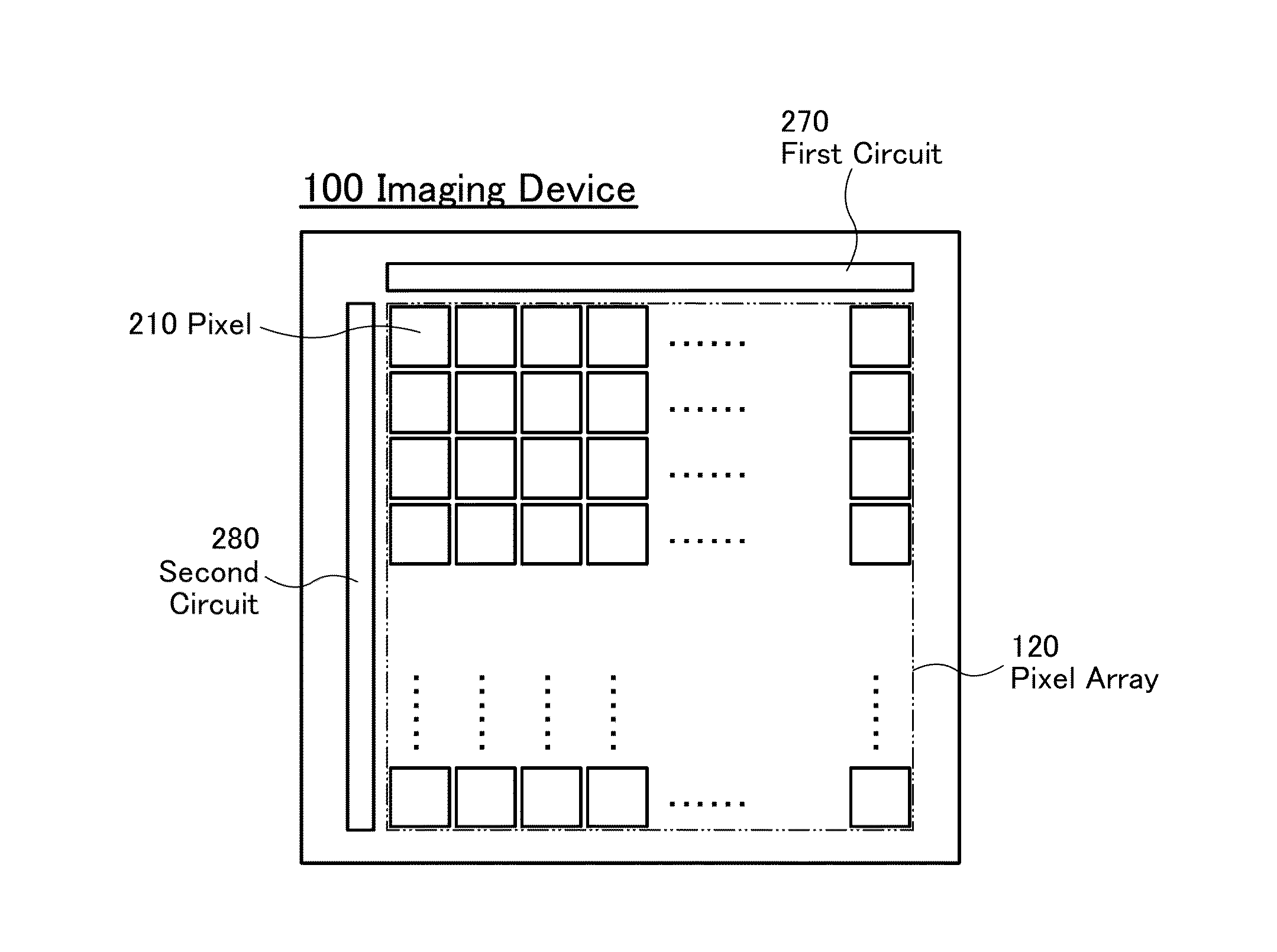
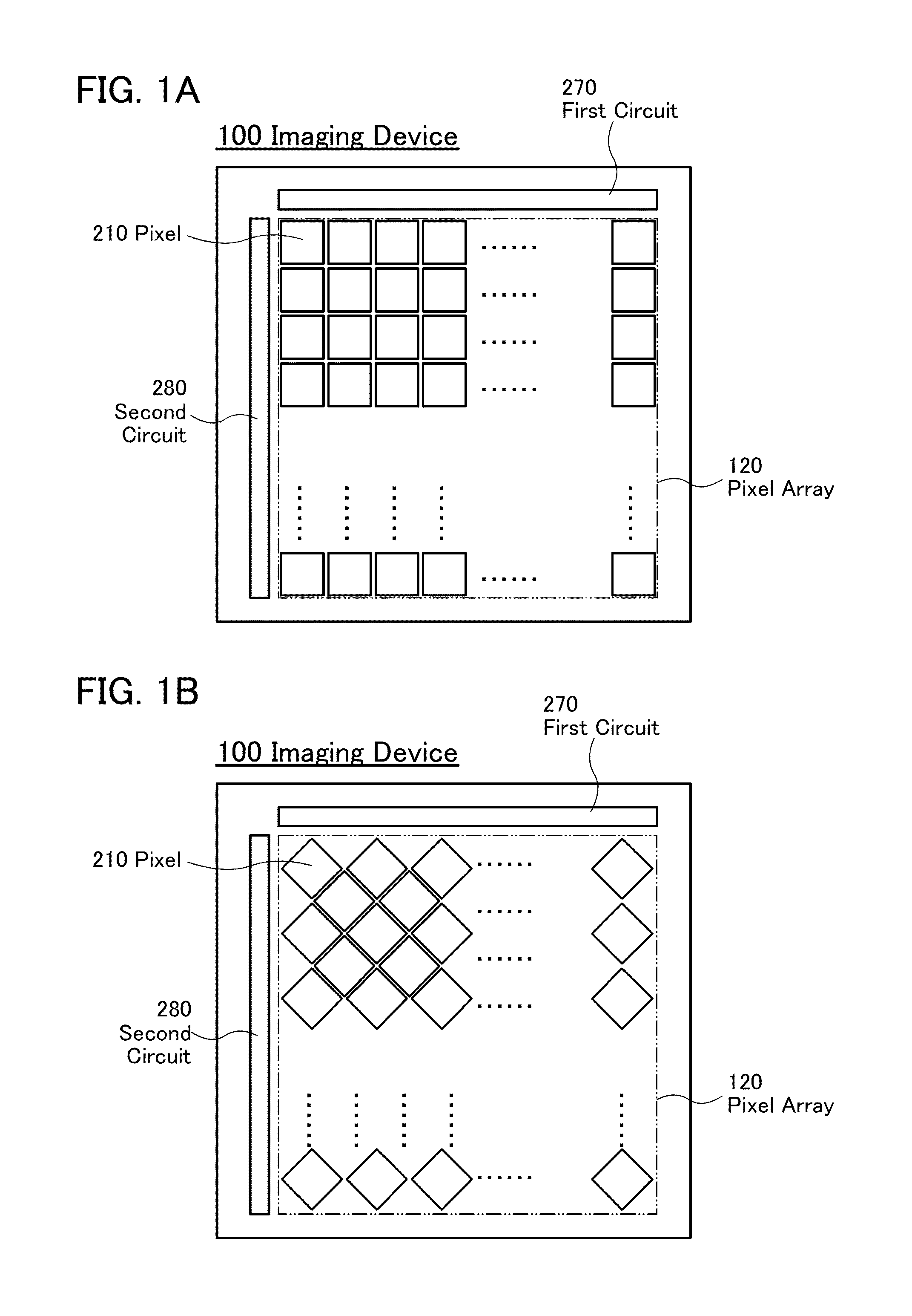
[0101]FIG. 1A is a plan view illustrating a configuration example of an imaging device 100 of one embodiment of the present invention. The imaging device 100 includes a pixel array 120 and a first and a second circuit 270 and 280 for driving the pixel array 120. The pixel array 120 includes a plurality of pixels 210 arranged in a matrix. The first circuit 270 and the second circuit 280 are connected to the plurality of pixels 210 and have a function of supplying signals for driving the pixels 210. Note that in this specification and the like, the first circuit 270, the second circuit 280, and the like are referred to as a peripheral circuit or a driver circuit in some cases. For example, the first circuit 270 is part of a peripheral circuit. The second circuit 280 is also part of a peripheral circuit.

[0102]As illustrated in FI...

Example

Embodiment 2

[0309]In this embodiment, an example of a circuit configuration that can be used for the pixel 210 and the operation of the imaging device 100 are described.

Example

Example 1 of Circuit Configuration

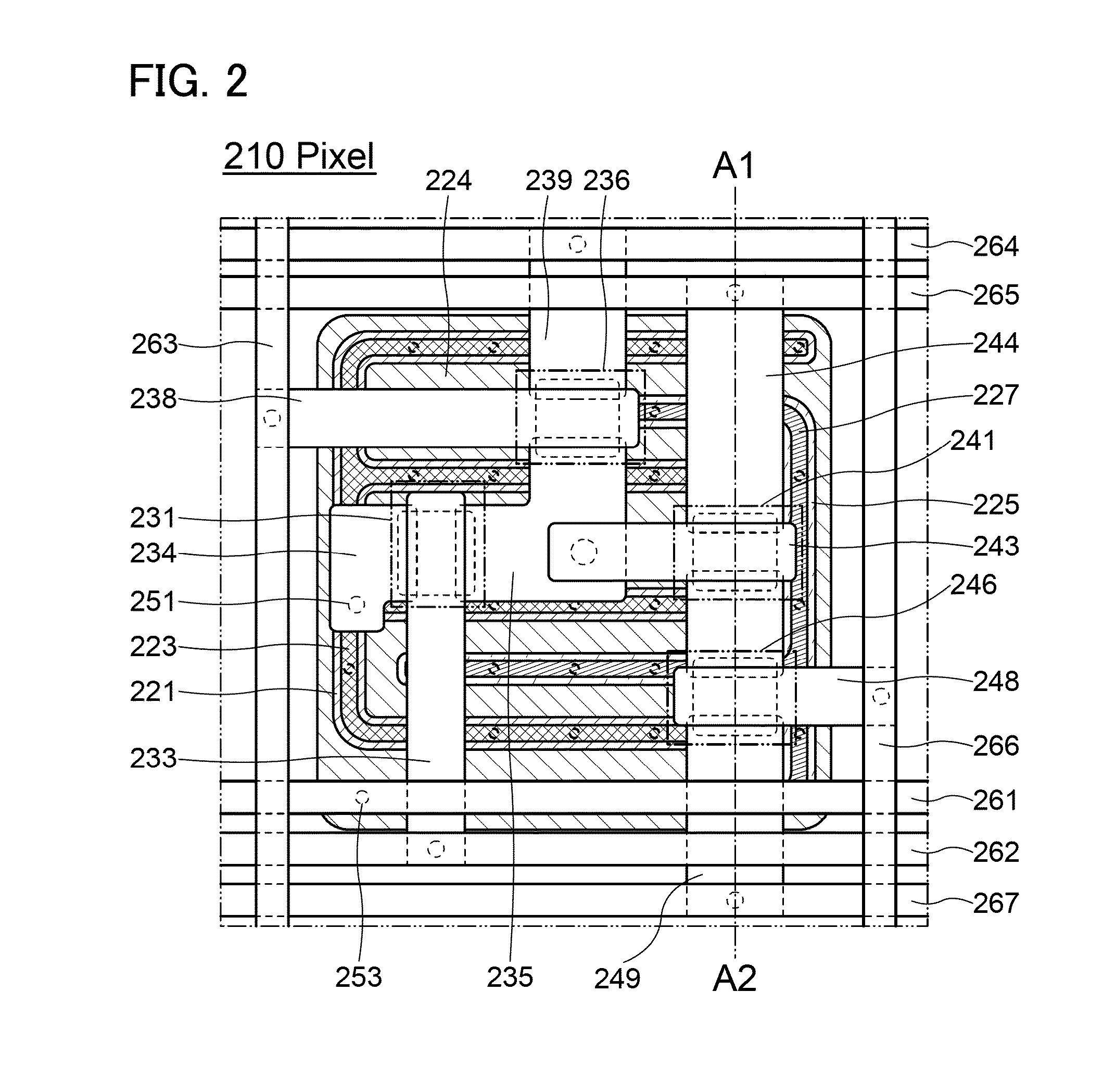
[0310]FIG. 10A illustrates an example of a circuit configuration that can be used for the pixel 210. A circuit 1000 in FIG. 10A includes a photodiode 1002 which is a photoelectric conversion element, a transfer transistor 1004, a reset transistor 1006, an amplifier transistor 1008, a wiring 1100, a wiring 1110, and a wiring 1120. A pixel array can be formed by arranging a plurality of circuits 1000 in a matrix.

[0311]The photodiode 1002 corresponds to the light-receiving element 220 described in the above embodiment, for example. The transfer transistor 1004 corresponds to the transistor 231, for example. The reset transistor 1006 corresponds to the transistor 236, for example. The amplifier transistor 1008 corresponds to the transistor 241, for example.

[0312]In the circuit 1000, the photodiode 1002 is electrically connected to one of a source and a drain of the transfer transistor 1004, and the other of the source and the drain of the transfer trans...


PUM


Abstract

An imaging device is provided at a lower manufacturing cost. In a light-receiving portion of an imaging device which includes the light-receiving portion, a first transistor connected to the light-receiving portion, and a peripheral circuit, a comb-like n-type semiconductor and a comb-like p-type semiconductor are arranged so as to engage with each other in a plan view. Further, the light-receiving portion and the first transistor overlap with each other. The peripheral circuit includes a second transistor and a third transistor. Further, the second transistor and the third transistor include semiconductor layers having different bandgaps. Further, one of the semiconductor layers of the second transistor and the third transistor has the same bandgap as a semiconductor layer of the first transistor.

Description

BACKGROUND OF THE INVENTION[0001]1. Field of the Invention[0002]One embodiment of the present invention relates to a semiconductor device. In particular, one embodiment of the present invention relates to a semiconductor device including an oxide semiconductor.[0003]Note that one embodiment of the present invention is not limited to the above technical field. For example, one embodiment of the present invention relates to an object, a method, or a manufacturing method. Further, one embodiment of the present invention relates to a process, a machine, manufacture, or a composition of matter. Further, one embodiment of the present invention relates to a memory device, a processor, a driving method thereof, or a manufacturing method thereof.[0004]In this specification and the like, a semiconductor device generally means a device that can function by utilizing semiconductor characteristics. Thus, a semiconductor element such as a transistor or a diode and a semiconductor circuit are semi...

Claims


Application Information

Patent Timeline
IPC IPC(8): H01L27/146H01L29/06
CPCH01L27/14616H01L29/0688H01L27/14607H01L27/14643H01L27/14609H01L27/14612H01L27/14641H01L27/14689H01L29/7869
Inventor YAMAZAKI, SHUNPEISAKAKURA, MASAYUKIKUROKAWA, YOSHIYUKI
Owner SEMICON ENERGY LAB CO LTD
Why Eureka
Try Eureka