Lift-off method

Active Publication Date: 2015-11-19
DISCO CORP
View PDF2 Cites 14 Cited by
  • Summary
  • Abstract
  • Description
  • Claims
  • Application Information

AI Technical Summary

Benefits of technology

[0018]As described above, the lift-off method of the present invention includes the transfer substrate bonding step of bonding the transfer substrate through the bonding layer to the front side of the optical device layer of the optical device wafer, thereby forming the composite substrate; the buffer layer breaking step of applying the pulsed laser beam having a wavelength transmissive to the epitaxy substrate and absorptive to the buffer layer from the back side of the epitaxy substrate to the buffer layer after performing the transfer substrate bonding step, thereby breaking the buffer layer; and the optical device layer transferring step of peeling the epitaxy substrate from the optical device layer after performing the buffer layer breaking step, thereby transferring the optical device layer to the transfer substrate, wh

Problems solved by technology

However, in applying the laser beam from the back side of the epitaxy substrate to the buffer layer in the condition where the focal point of the laser beam is set in the buffer layer, thereby breaking the buffer layer, there is a case that the buffer layer cannot be sufficiently broken, causing a problem such that the epitaxy substrate cannot be smoothly peeled off.
Further, in the case that

Method used


Image

  • Lift-off method
  • Lift-off method
  • Lift-off method

Examples


Example

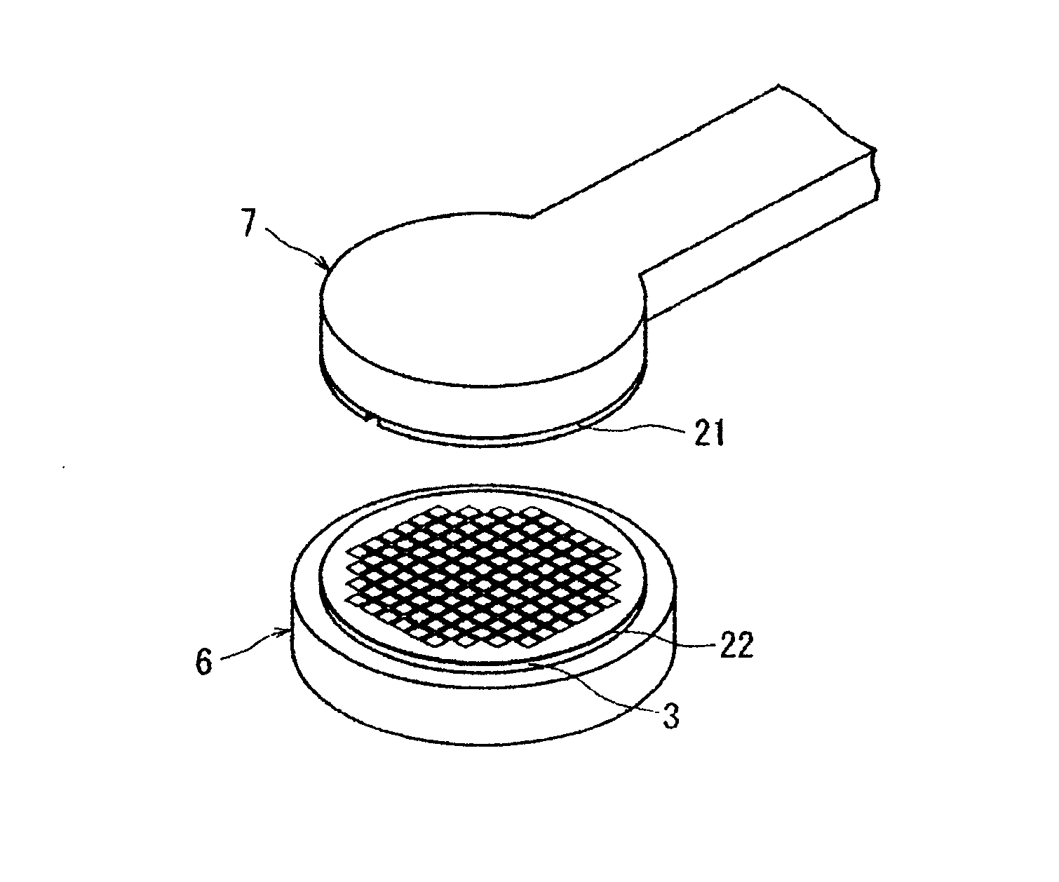
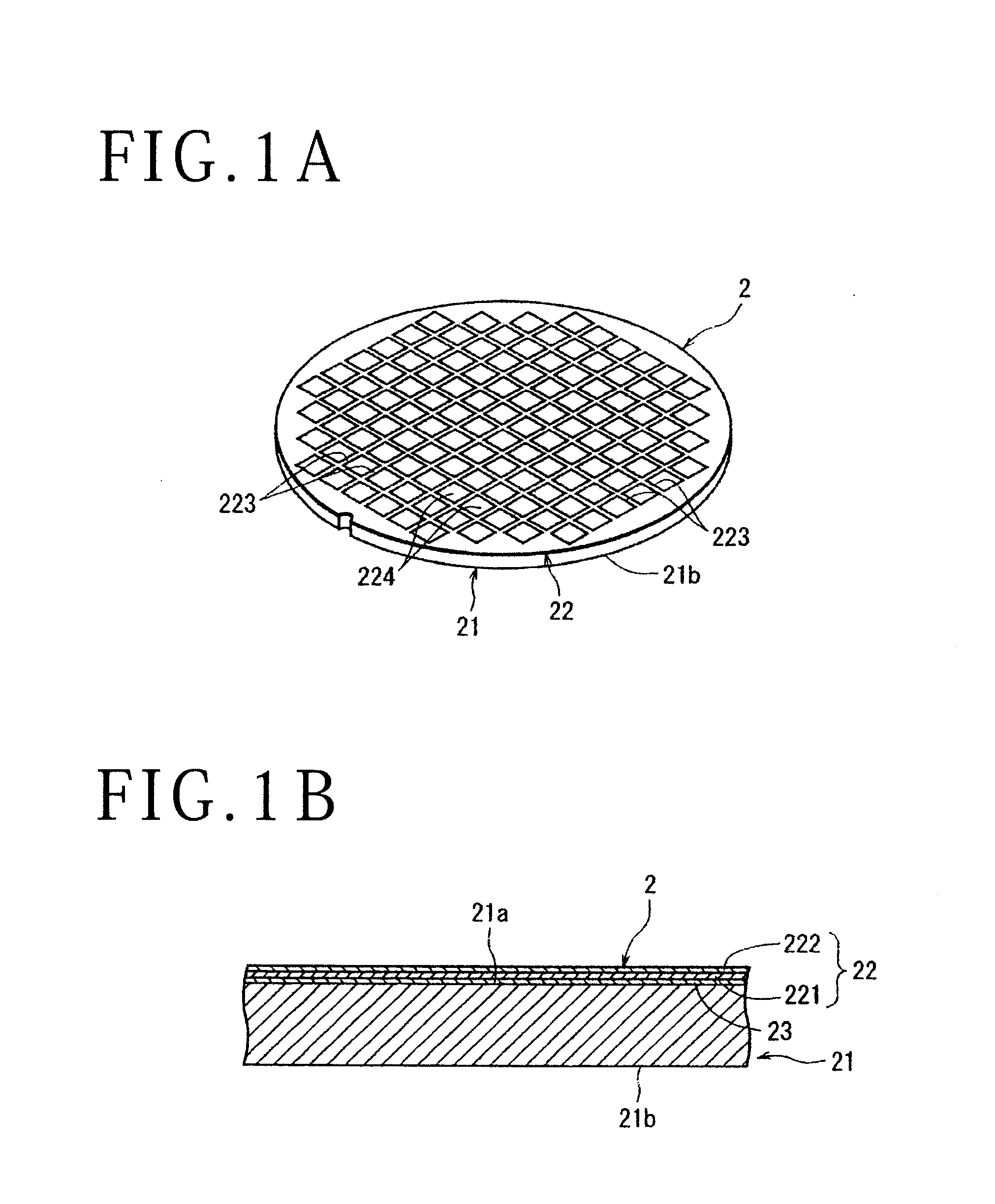
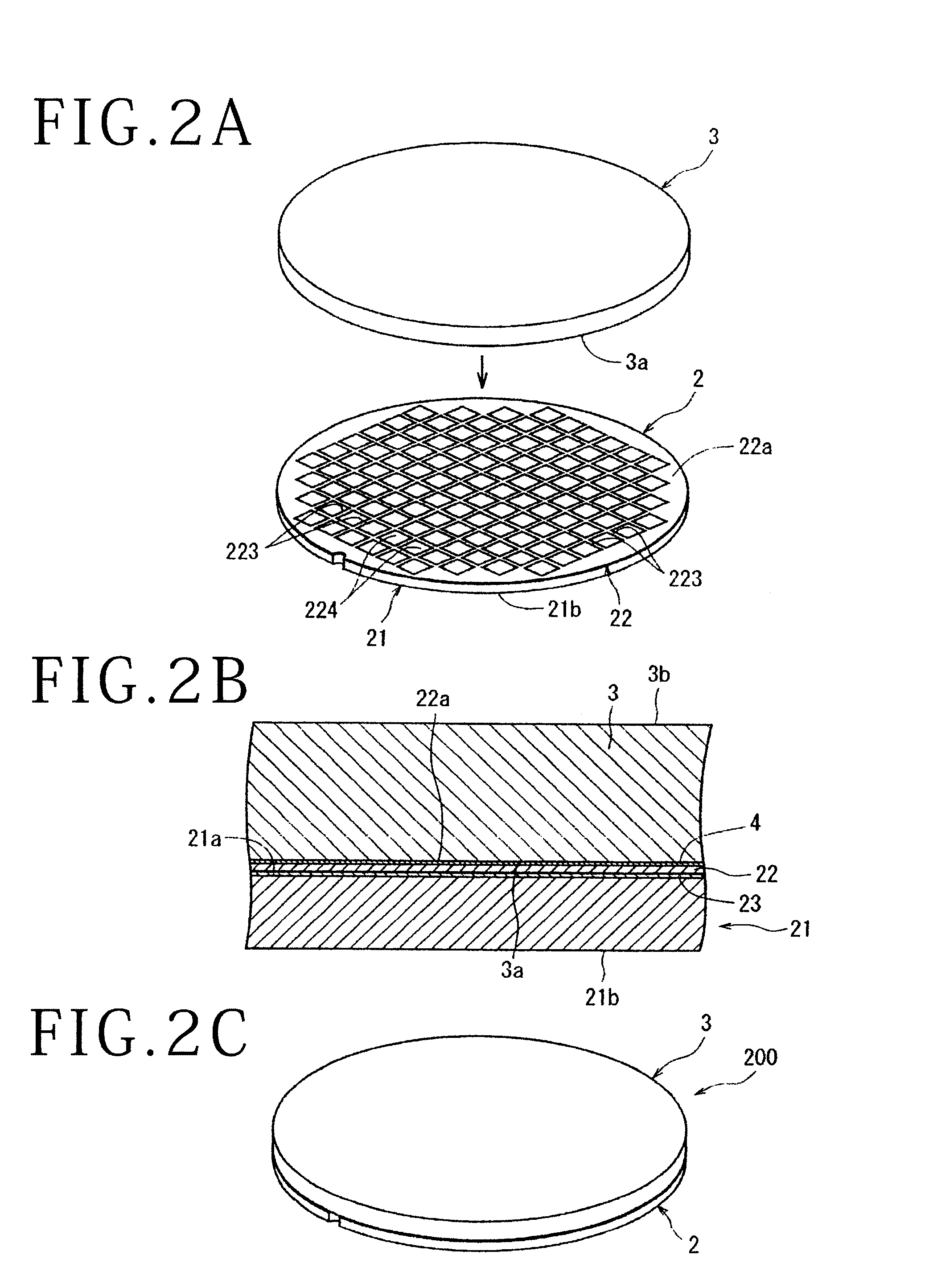
[0035]Preferred embodiments of the lift-off method according to the present invention will now be described in detail with reference to the attached drawings. FIG. 1A is a perspective view of an optical device wafer 2 having an optical device layer to be transferred to a transfer substrate by the lift-off method according to the present invention, and FIG. 1B is an enlarged sectional view of an essential part of the optical device wafer 2 shown in FIG. 1A.

[0036]The optical device wafer 2 shown in FIGS. 1A and 1B is formed by epitaxial growth of an optical device layer 22 on the front side 21a of a circular epitaxy substrate 21. The epitaxy substrate 21 is formed from a sapphire substrate. The epitaxy substrate 21 has a diameter of 50 mm and a thickness of 600 μm, for example. The optical device layer 22 is composed of an n-type gallium nitride semiconductor layer 221 and a p-type gallium nitride semiconductor layer 222. In forming the optical device layer 22 composed of the n-type g...


PUM

PropertyMeasurementUnit
Frequencyaaaaaaaaaa

Abstract

A lift-off method for transferring an optical device layer in an optical device wafer to a transfer substrate, the optical device layer being formed on the front side of an epitaxy substrate through a buffer layer. A transfer substrate is bonded through a bonding layer to the front side of the optical device layer of the optical device wafer, thereby forming a composite substrate. A pulsed laser beam having a wavelength transmissive to the epitaxy substrate and absorptive to the buffer layer is applied from the back side of the epitaxy substrate to the buffer layer, thereby breaking the buffer layer, and the epitaxy substrate is peeled from the optical device layer, thereby transferring the optical device layer to the transfer substrate. Ultrasonic vibration is applied to the composite substrate in transferring the optical device layer.

Description

BACKGROUND OF THE INVENTION[0001]1. Field of the Invention[0002]The present invention relates to a lift-off method for transferring an optical device layer in an optical device wafer to a transfer substrate, the optical device layer being formed on the front side of an epitaxy substrate such as a sapphire substrate and a silicon carbide substrate through a buffer layer.[0003]2. Description of the Related Art[0004]In an optical device fabrication process, an optical device layer composed of an n-type semiconductor layer and a p-type semiconductor layer is formed on the front side of a substantially disk-shaped epitaxy substrate such as a sapphire substrate and a silicon carbide substrate through a buffer layer. The optical device layer is formed of GaN (gallium nitride), for example. The optical device layer is partitioned by a plurality of crossing streets into a plurality of regions where a plurality of optical devices such as light emitting diodes and laser diodes are formed, thus...

Claims


Application Information

Patent Timeline
IPC IPC(8): B32B37/00H01L33/00B32B43/00H01L21/683
CPCB32B37/025H01L21/6835H01L33/0079B32B43/006H01L2221/6839B32B2551/00B32B2307/40B32B2310/028B32B2310/0843B32B2310/0409H01L2221/68363H01L21/7813B23K20/002B23K20/10B23K26/0853B23K26/50B23K26/0624H01L21/2007B23K2101/40B23K2103/56B23K2103/172H01L21/78H01L33/0093
Inventor KOYANAGI, TASUKUTAKEDA, NOBORUMORIKAZU, HIROSHI
Owner DISCO CORP
Why Eureka
Try Eureka