Methods and Systems for Fabricating High Quality Superconducting Tapes
a superconducting tape and superconducting technology, applied in the direction of superconducting magnets/coils, magnetic bodies, superconductor devices, etc., can solve the problems of significantly deteriorating the superconducting quality of the tape, poor surface microstructure, and unfavorable superconducting quality, so as to reduce the amount of misoriented grain growth, reduce the amount of precursor to film, and reduce the effect of oxidation
- Summary
- Abstract
- Description
- Claims
- Application Information
AI Technical Summary
Benefits of technology
Problems solved by technology
Method used
Image
Examples
example 1
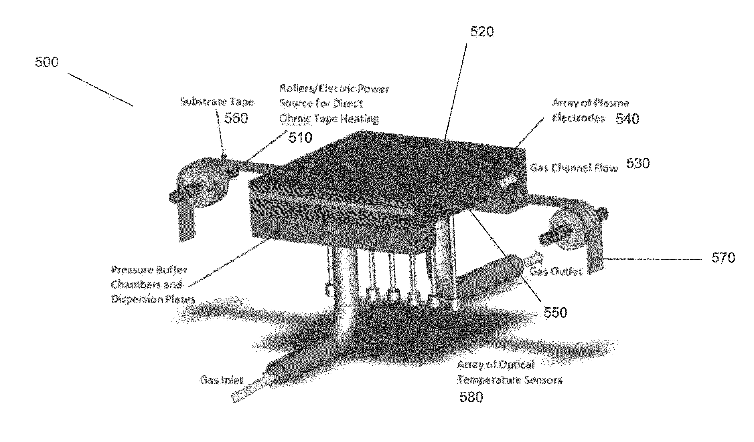
[0040]FIG. 7, by way of example only, displays the current-voltage characteristics (i.e. critical current density) of a 1.8 μm thick REBa2Cu3O7 film. The film was fabricated in an improved MOCVD system, such as the embodiment described in FIGS. 5A-5B. The data shows that the tape has a critical current at 916 A over a 12 mm width, at 77 K in a zero applied magnetic field, which corresponds to a current density at 4.24 MA / cm2. This is a substantially high current density for an MOCVD-fabricated superconductor tape with thickness greater than 1 μm.
example 2
[0041]FIG. 8 illustrates the surface microstructure of a 2 μm thick REBa2Cu3O7 film. The film was fabricated in an improved MOCVD system, such as the embodiment described in FIGS. 5A-5B. The tape is substantially uniform with no observable misoriented grain growth.
example 3
[0042]FIG. 9A illustrates a surface microstructure of a 3.2 μm thick REBa2Cu3O7 film. The film was fabricated in an improved MOCVD system, such as the embodiment described in FIGS. 5A-5B. The tape is substantially uniform with no observable misoriented grain growth. There are some secondary phases relegated to the surface. FIG. 9B shows a cross section microstructure of the same 3.2 μm thick REBa2Cu3O7 film. The cross-section is substantially homogenous and also shows no misoriented grain growth. FIG. 9C shows 2-D X-ray Diffraction data for the 3.2 μm thick REBa2Cu3O7 film. Again, this data shows that the film lacks misoriented grain growth (i.e. no diffraction spots corresponding to non (001) orientation, perpendicular to the central horizontal axis). The data further reveals the presence of grains only along the c-axis (i.e. diffraction spots along the central horizontal axis).
PUM
| Property | Measurement | Unit |
|---|---|---|
| temperature | aaaaa | aaaaa |
| temperature | aaaaa | aaaaa |
| thickness | aaaaa | aaaaa |
Abstract
Description
Claims
Application Information


