Stable metal-oxide thin film transistor and method of making

a thin film transistor and metal oxide technology, applied in the direction of transistors, semiconductor devices, electrical appliances, etc., can solve the problems of oxides with large crystalline grains, current dilemma or trade, and the inability to stabilize metal oxide semiconductors, so as to improve stability, improve the effect of stability and good control of oxygen vacancies

Inactive Publication Date: 2015-12-10
YU GANG +5
View PDF3 Cites 35 Cited by
  • Summary
  • Abstract
  • Description
  • Claims
  • Application Information

AI Technical Summary

Benefits of technology

[0013]Another object of the invention is to provide a new and improved metal oxide semiconducto

Problems solved by technology

However, a major deficiency of metal oxide semiconductors is stability and the tendency to become polycrystalline at higher temperatures.
Polycrystalline semiconductor metal oxides with large crystalline grains (e.g., approaching micron grain size) are not desirable in semiconductor devices for several reasons.
Therefore, there is currently a dilemma or trade-off between the selection of etch-stop type or BCE type of metal-oxide TFTs for manufacturing.
The diffusion of hydrogen from the gate insulator into the metal oxide channel usually causes serious deterior

Method used


Image

  • Stable metal-oxide thin film transistor and method of making
  • Stable metal-oxide thin film transistor and method of making
  • Stable metal-oxide thin film transistor and method of making

Examples


Embodiment Construction

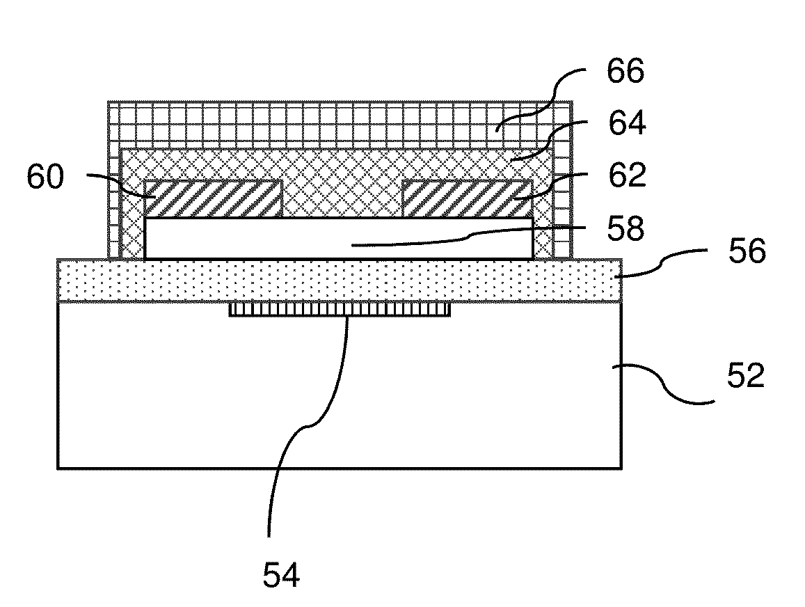
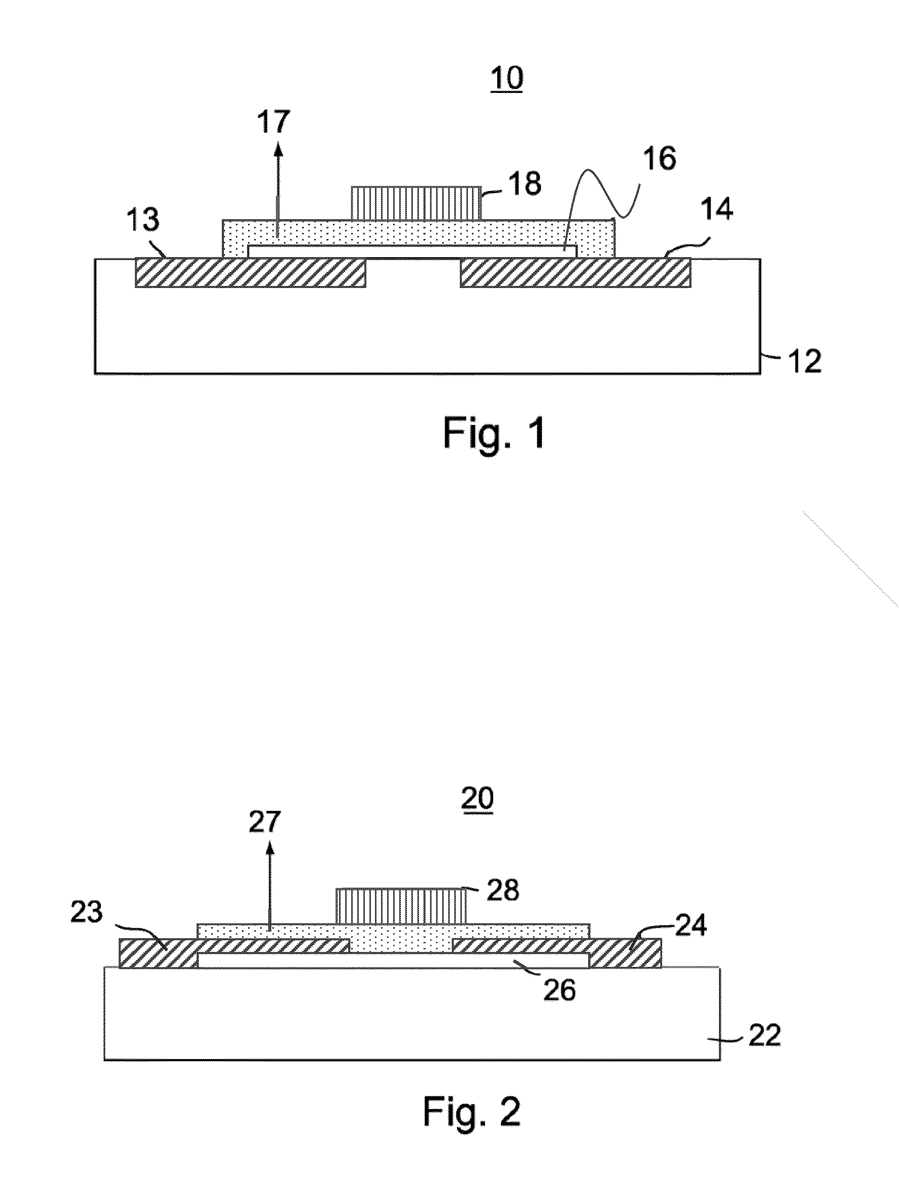
[0031]Turning now to FIG. 1, a simplified layer diagram of one embodiment of a TFT 10, in accordance with the present invention, is illustrated. TFT 10 includes a substrate 12, which may be a flexible material, such as plastic, stainless-steel, or any other convenient material, such as glass, etc. A source 13 and a drain 14 are formed in or on (hereinafter generically referred to as “on”) the upper surface of substrate 12 in a spaced apart orientation using any well-known method. A metal oxide semiconductor film 16 is formed in partial overlying relationship to both source 13 and drain 14 and the space therebetween. It will be understood that metal oxide semiconductor film 16 is the active layer that conducts carriers between the source / drain components. In a preferred embodiment, metal oxide layer 16 is less than 100 nm thick and preferably less than 50 nm. A thin gate dielectric layer 17 is formed in overlying relationship to metal oxide film 16 and a gate stack 18 is positioned o...


PUM


Abstract

A thin film semiconductor device has a semiconductor layer including a composite/blend/mixture of an amorphous/nanocrystalline semiconductor ionic metal oxide and an amorphous/nanocrystalline non-semiconducting covalent metal oxide. A pair of terminals is positioned in communication with the semiconductor layer and define a semiconductive channel, and agate terminal is positioned in communication with the semiconductive channel and further positioned to control conduction of the channel. The invention further includes a method of depositing the mixture including using nitrogen during the deposition process to control the carrier concentration in the resulting semiconductor layer.

Description

CROSS-REFERENCE TO RELATED APPLICATIONS[0001]This application is a continuation-in-part application of currently pending U.S. application Ser. No. 12 / 206,615, filed Sep. 8, 2008.FIELD OF THE INVENTION[0002]This invention relates to metal oxide semiconductor material for use in channel layers of semiconductor devices, especially in the back channel etch (BCE) type of thin film transistor (TFT) devices.BACKGROUND OF THE INVENTION[0003]In thin film semiconductor devices such as thin film transistors (TFTs), the devices include spaced apart source and drain areas that conduct through a channel layer positioned therebetween. At least one gate insulator and gate electrode are positioned above and / or below the channel layer, to control the conduction. In many applications TFTs are used where high heat cannot be tolerated during fabrication and, thus, a semiconductor must be used that can be deposited at relatively low temperatures (e.g. room temperature) but which still has relatively high...

Claims


Application Information

Patent Timeline
IPC IPC(8): H01L29/786H01L21/28H01L29/49H01L29/66H01L29/417H01L29/423H01L21/283H01L21/324
CPCH01L29/78693H01L21/283H01L21/28008H01L21/324H01L29/78603H01L29/41733H01L29/42384H01L29/42364H01L29/4908H01L29/66742H01L21/02554H01L21/02565H01L21/02592H01L29/7869H10K10/471
Inventor YU, GANGSHIEH, CHAN-LONGXIAO, TIANFOONG, FATTMUSULF, JUERGENOTTOSSON, KARL BIRGER KRISTOFFER
Owner YU GANG
Why Eureka
Try Eureka