Systems and methods for implementing digital vapor phase patterning using variable data digital lithographic printing techniques

a digital lithographic printing and variable data technology, applied in the direction of railway signalling, transportation and packaging, nuclear engineering, etc., can solve the problems of metals onto the substrate surface, inability to accurately and positively jet inkjet process, and complex number of steps, so as to increase the alignment fidelity of images transferred, reduce alignment errors, and facilitate the effect of implementation

Inactive Publication Date: 2015-12-31
PALO ALTO RES CENT INC
View PDF5 Cites 12 Cited by
  • Summary
  • Abstract
  • Description
  • Claims
  • Application Information

AI Technical Summary

Benefits of technology

[0030]Exemplary embodiments may provide a dynamic process by which to modify the oil layer release pattern on each pass providing an additional degree of freedom in the patterning process.
[0031]Exemplary embodiments may employ laser evaporation of the oil layer to provide an ability to do short-run patterning on-the-fly making it easier to implement, for example, different circuit geometries in a particular manufacturing run, thereby providing added flexibility.
[0032]E

Problems solved by technology

As shown in the above example of a conventional patterning process, such as a patterning technique for semiconductor substrates, metals or other layered products, require a complex and complicated number of steps to accomplish the patterning of the layer of material.
While inkjet provides an avenue by which to accomplish this in certain restricted scenarios, the inkjet process suffers from

Method used


Image

  • Systems and methods for implementing digital vapor phase patterning using variable data digital lithographic printing techniques
  • Systems and methods for implementing digital vapor phase patterning using variable data digital lithographic printing techniques
  • Systems and methods for implementing digital vapor phase patterning using variable data digital lithographic printing techniques

Examples


Embodiment Construction

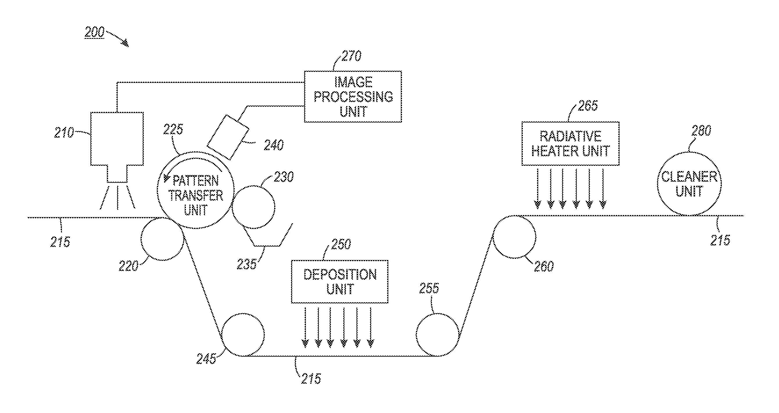
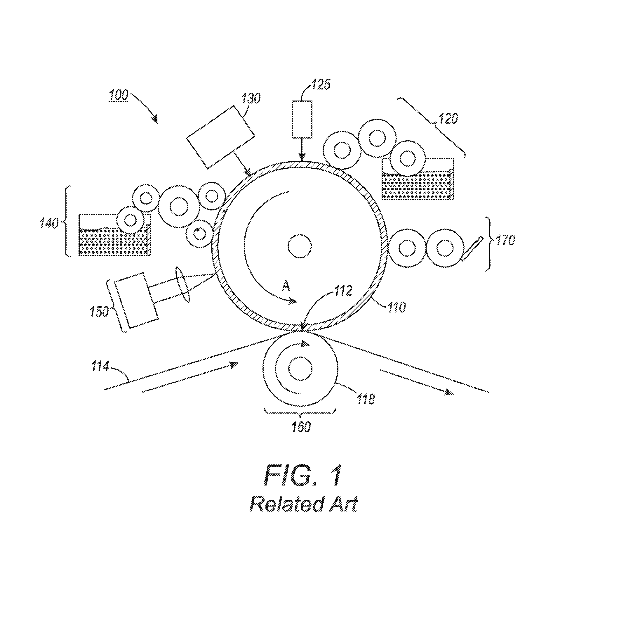
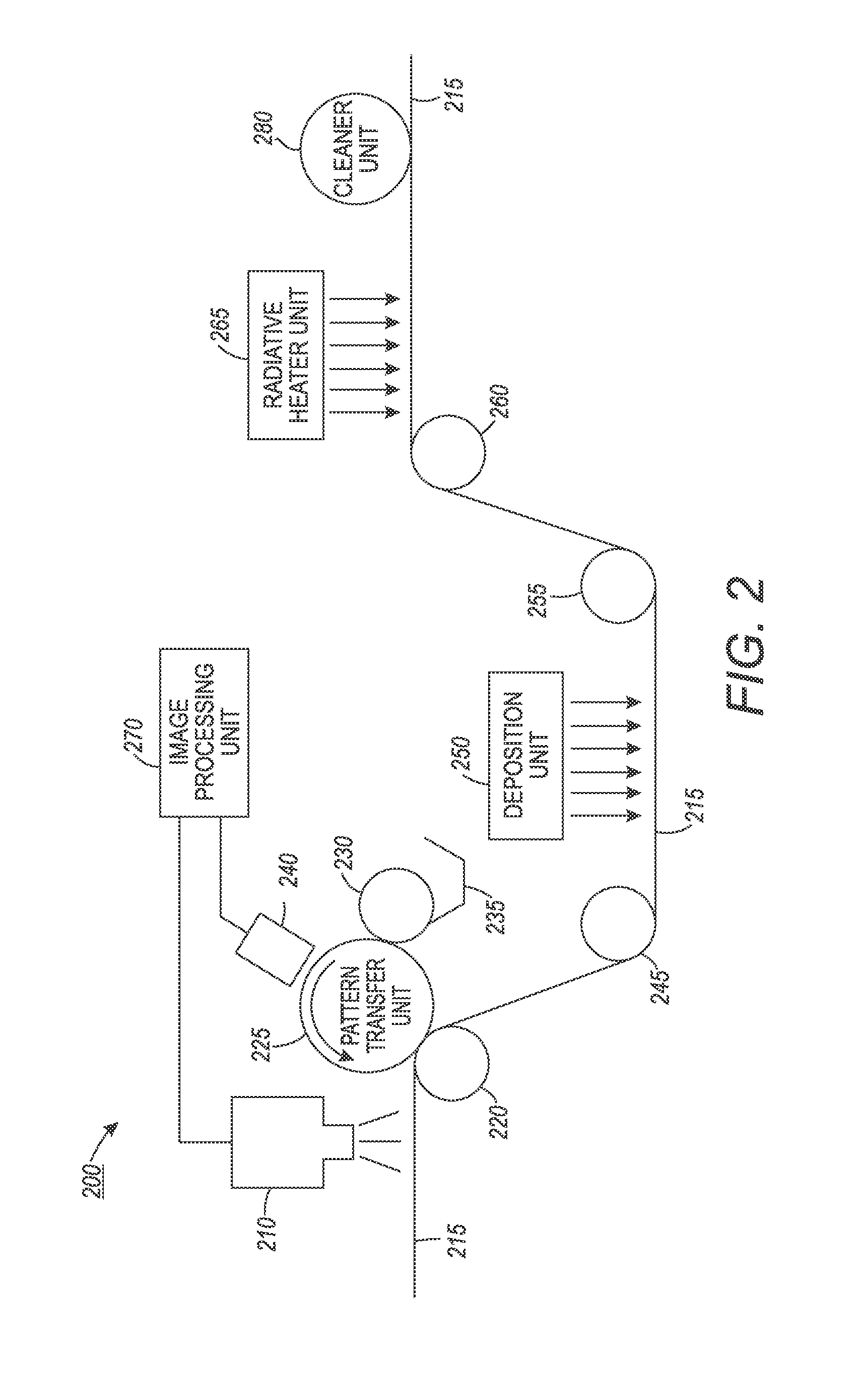
[0012]U.S. Patent Application Publication No. 2012 / 0103212 A1 (the 212 Publication) published May 3, 2012 and based on U.S. patent application Ser. No. 13 / 095,714, which is commonly assigned and the disclosure of which is incorporated by reference herein in its entirety, proposes systems and methods for providing variable data lithographic and offset lithographic printing or image receiving medium marking. The systems and methods disclosed in the 212 Publication are directed to improvements on various aspects of previously-attempted variable data digital imaging lithographic marking concepts based on variable patterning of dampening solutions to achieve effective truly variable digital data lithographic image forming.

[0013]The 212 Publication describes, in requisite detail, an exemplary variable data lithography system 100 such as that shown, for example, in FIG. 1. A general description of the exemplary system 100 shown in FIG. 1 is provided here. Additional details regarding indiv...


PUM

PropertyMeasurementUnit
Material propertiesaaaaaaaaaa

Abstract

A system and method are provided for implementing a unique scheme by which to execute digital vapor phase patterning on metals, semiconductor substrates and other surfaces using a proposed variable data digital lithographic image forming architecture or technique. For certain substrate printing and manufacturing applications, including some printed electronics applications, the disclosed schemes implement techniques to digitally pattern metal layers with bulk material properties in a manner that is aligned with underlying layers on the fly. The disclosed digital printing process may pattern a release oil on a substrate in support of a metal deposition process. Changeable patterning is implemented with an ability to modify the alignment of the patterns on-the-fly. The release layer on a drum is laser patterned in order that the patterned release layer is transferred to the substrate, or the patterning of the release layer is accomplished directly on the substrate.

Description

BACKGROUND[0001]1. Field of Disclosed Subject Matter[0002]This disclosure relates to systems and methods that provide unique techniques by which to implement digital vapor phase patterning on metals, semiconductor substrates and other surfaces using a proposed variable data digital lithographic image forming architecture.[0003]2. Related Art[0004]For a decade or so, it has been well known in certain fields, including in the manufacture of semiconductor devices, to deposit and patterned thin layers to a number of beneficial results, including the patterning of certain semiconductor devices. Variations in the deposition and patterning steps define the function of the manufactured device and a density of individually patterned elements on the substrate.[0005]A common patterning method for the deposited layers involves an optical patterning, and using related processes. In a photolithographic process, for example, a substrate coated with a photosensitive resist layer deposited thereon i...

Claims


Application Information

Patent Timeline
IPC IPC(8): C23C14/24C23C14/28
CPCC23C14/042C23C14/562C23C14/54C23C14/56C23C14/5873
Inventor VERES, JANOSSTOWE, TIMOTHY D.WHITING, GREGORY
Owner PALO ALTO RES CENT INC
Why Eureka
Try Eureka