Semiconductor device with a vertical channel

a technology of vertical channel and semiconductor, applied in the direction of semiconductor devices, electrical equipment, transistors, etc., can solve the problems of increasing processing cost, gate voltage cannot be scaled, and channel length is limited by lithography capabilities

Active Publication Date: 2016-01-07
AVAGO TECH INT SALES PTE LTD
View PDF6 Cites 36 Cited by
  • Summary
  • Abstract
  • Description
  • Claims
  • Application Information

AI Technical Summary

Problems solved by technology

This channel length is limited by lithography capabilities.
The channel length of 20 nm can be achieved using double or multiple patterning, which is expensive as multiple patterning increases the processing cost.
However, because of gate capacitance coupling, the gate voltage cannot be scaled as the channel length gets scaled.
However, this gate voltage cannot get smaller than a limit that is forced by gate capacitive coupling in a conventional lateral transistor.
Also, smaller channel lengths can result in increased source/drain leakage in the off state.
Further, a small channel length can cause drain-induced barrier lowering (DIBL) effect that can result in premature turning on of the transistor when a high drain voltage is applied.
Additionally, there are multiple manufacturing challenges with conventional methods for making the channel length smaller, these manufacturing challenges include channel doping uniformity, line edge roughness, and

Method used


Image

  • Semiconductor device with a vertical channel
  • Semiconductor device with a vertical channel
  • Semiconductor device with a vertical channel

Examples


Embodiment Construction

Overview

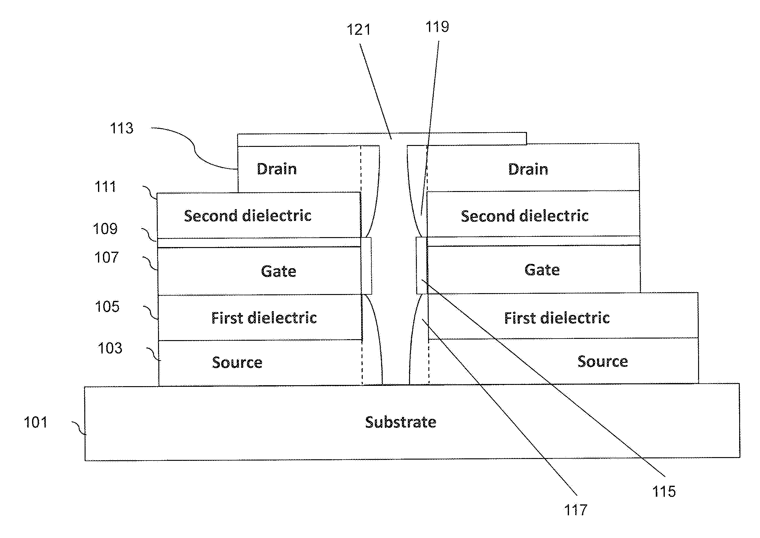
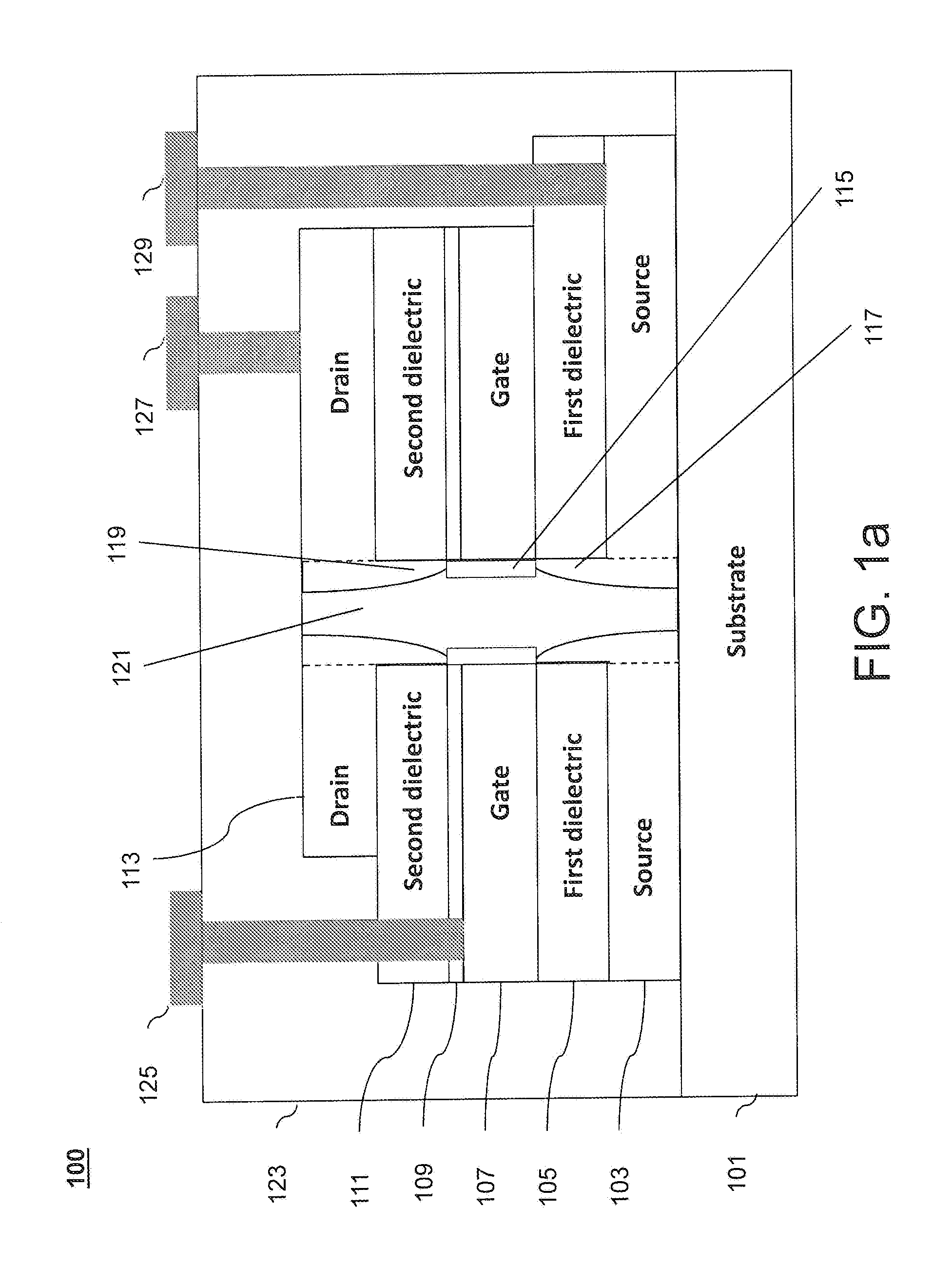
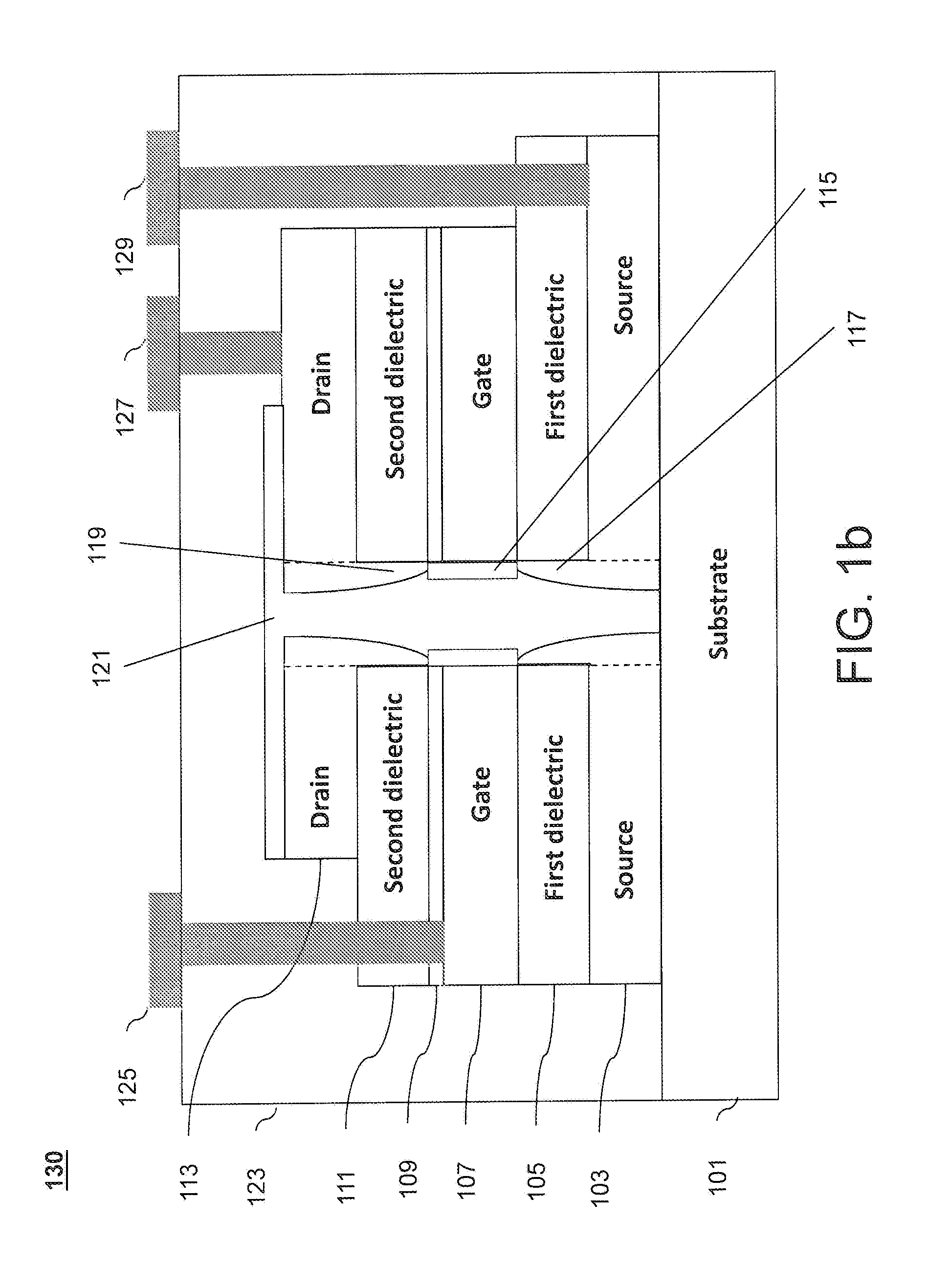
[0019]Semiconductor devices and manufacturing methods are provided for making channel and gate lengths independent of lithography limitations, which enables: smaller device feature scaling, better control of short-channel effect, reduced substrate implantation sensitivity, higher drive current per silicon area resulting in faster switching speed, and the ability to decouple device packing density from gate length. Semiconductor devices and manufacturing methods are provided for increasing resistivity between drain and channel to allow for higher voltage operation.

[0020]According to one embodiment of the disclosure, a semiconductor device includes a first doped layer implanted in a semiconductor substrate forming one of a source or a drain and a gate metal layer disposed over the first doped layer. The semiconductor device further includes a second doped layer disposed over the gate metal forming the other the source or the drain, where the first doped layer, the gate metal l...


PUM


Abstract

Semiconductor devices and manufacturing methods are provided for making channel and gate lengths independent from lithography. Also, semiconductor devices and manufacturing methods are provided for increasing resistivity between drain and channel to allow for higher voltage operation. For example, a semiconductor device includes a first doped layer implanted in a semiconductor substrate forming one of a source or a drain and a gate metal layer disposed over the first doped layer. The semiconductor device further includes a second doped layer disposed over the gate metal forming the other the source or the drain, where the first doped layer, the gate metal layer and the second doped layer form a vertical stack of layers of the semiconductor device. The semiconductor device further includes a conduction channel formed in a trench that extends vertically through the vertical stack of layers and terminates at the semiconductor substrate.

Description

CROSS REFERENCE TO RELATED APPLICATIONS[0001]The present application claims the benefit of U.S. Provisional Patent Application No. 62 / 020,960 filed on Jul. 3, 2014, which is hereby incorporated by reference in its entirety.BACKGROUND[0002]1. Field[0003]The present disclosure relates generally to semiconductor devices with vertical channels and methods of making them.[0004]2. Background Art[0005]In a conventional silicon transistor that includes a source, a gate, and a drain, channel length (LG) is the length between the source to the drain inside a silicon substrate. This channel length is limited by lithography capabilities. In conventional methods, the channel length can be no smaller than 28 nm or 20 nm. The channel length of 20 nm can be achieved using double or multiple patterning, which is expensive as multiple patterning increases the processing cost. As the need for smaller semiconductors increases, there is a need to make the channel length even smaller than 20 nm. As the c...

Claims


Application Information

Patent Timeline
IPC IPC(8): H01L29/78H01L29/10
CPCH01L29/1037H01L29/781H01L29/0865H01L29/0882H01L29/1033H01L29/78H01L29/7816H01L29/66666H01L29/7827H01L29/0653H01L29/0843H01L29/66712H01L29/7809
Inventor ZHAO, SAM ZIQUNHUI, FRANK
Owner AVAGO TECH INT SALES PTE LTD
Why Eureka
Try Eureka