Nitride semiconductor structure

a technology of nitride and semiconductors, applied in the field of nitride semiconductor structures, can solve the problems of obviating the generation of defects, cracking of thin films, and formation of defects, and achieve the effect of reducing the rupture of wafers

Inactive Publication Date: 2016-01-21
EPISIL PRECISION INC
View PDF5 Cites 3 Cited by
  • Summary
  • Abstract
  • Description
  • Claims
  • Application Information

AI Technical Summary

Benefits of technology

[0007]The disclosure is directed to a nitride semiconductor substructure, in which the incompatibilities of lattices and thermal expansion coefficients between a nitride semiconductor layer and a silicon substrate are improved to reduce the rupture of wafers and obviate the generation of defects.
[0028]According to the nitride semiconductor structure of the disclosure, through the disposition of the silicon carbide nucleation layer and the composite buffer layer, the incompatibilities of the lattices and the thermal expansion coefficients between gallium nitride and silicon are improved to overcome the problem of excessive defects present between the two. Moreover, the conventional nitride semiconductor structure typically includes aluminium nitride, and the epitaxy process time in forming aluminium nitride by MOCVD is long, resulting in a low throughput of the equipment. According to the disclosure, a nitride semiconductor structure, which is aluminium nitride free, is provided; hence, the epitaxy process time is reduced and the frequency of preventive maintenance of the equipment is also reduced.

Problems solved by technology

Aside from creating a rupture on the thin film due to the excessive thermal stress generated during the cooling period, the above differences may also generate internal strain in the gallium nitride semiconductor layer during the epitaxy process, resulting in a cracking of the thin film and a formation of defects.
Accordingly, resolving the incompatibilities of lattices and thermal expansion coefficients between a nitride semiconductor layer and a silicon substrate to mitigate the rupture of wafers and to obviate the generation of defects is still an issue for the industry to endeavour.

Method used


Image

  • Nitride semiconductor structure
  • Nitride semiconductor structure
  • Nitride semiconductor structure

Examples


Embodiment Construction

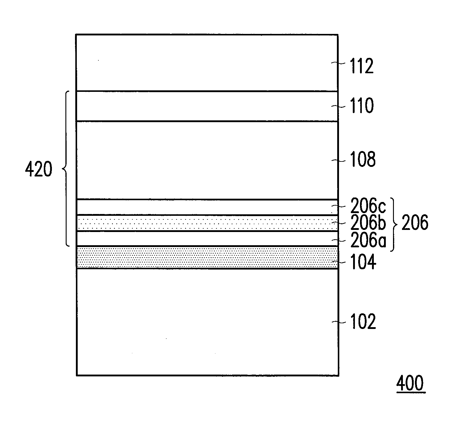
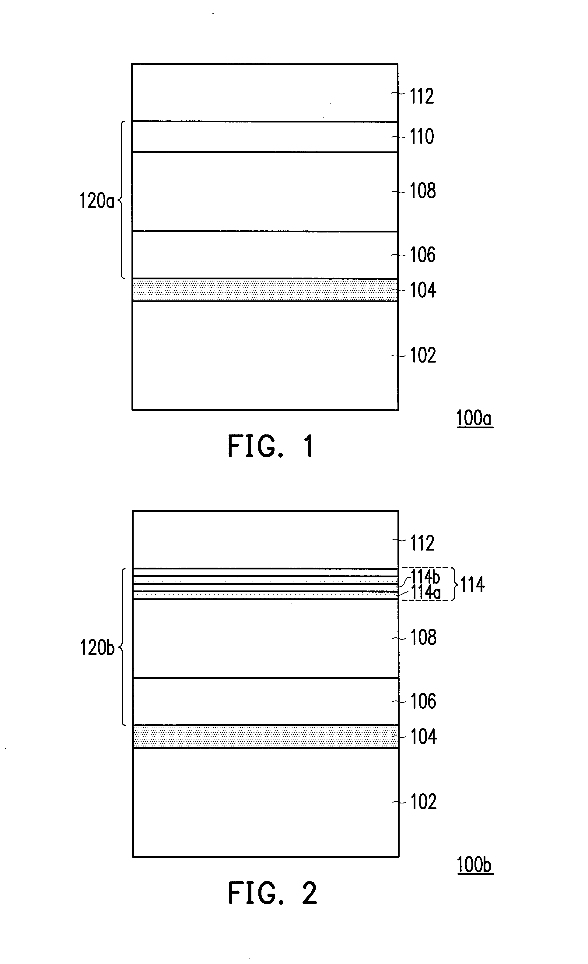
[0037]FIG. 1 is a schematic cross-sectional view of a nitride semiconductor structure of an exemplary embodiment of the disclosure. FIG. 2 is a schematic cross-sectional view of a nitride semiconductor structure of another exemplary embodiment of the disclosure.

[0038]Referring to FIG. 1, a nitride semiconductor structure 100a of the disclosure includes a substrate 102, a silicon carbide nucleation layer 104, a composite buffer layer 120a and a nitride semiconductor layer 112. The material of the substrate 102 includes, but is not limited to, silicon, aluminium oxide (Al2O3) or glass. In one exemplary embodiment, the substrate 102 can be a silicon substrate, wherein its crystal orientation is (111). The substrate 102 may be a patterned substrate, for example, a patterned silicon substrate. The patterns of the silicon substrate may be regular or irregular micro-patterns or nano-patterns. In one exemplary embodiment, the substrate 102, after being patterned, includes a plurality of rec...


PUM

PropertyMeasurementUnit
thicknessaaaaaaaaaa
thicknessaaaaaaaaaa
thicknessaaaaaaaaaa

Abstract

A nitride semiconductor structure is provided. The nitride semiconductor structure includes a substrate, a SiC nucleation layer, a composite buffer layer and a nitride semiconductor layer. The SiC nucleation layer is located on the substrate. The composite buffer layer is located on the SiC nucleation layer. The nitride semiconductor layer is located on the composite buffer layer. Besides, the nitride semiconductor structure is an AlN free semiconductor structure.

Description

CROSS REFERENCE TO RELATED APPLICATION[0001]This application claims the priority benefit of Taiwan application serial no. 103124565, filed on Jul. 17, 2014. The entirety of the above-mentioned patent application is hereby incorporated by reference herein and made a part of specification.BACKGROUND OF THE INVENTION[0002]1. Technical Field[0003]The disclosure generally relates to a semiconductor structure, and, more particularly, to a nitride semiconductor structure.[0004]2. Description of Related Art[0005]In recent years, nitride photodiodes have been broadly used in various fields. In a nitride semiconductor structure, since the silicon substrate bears the merits of high thermal conductivity and low cost, a large dimension nitride semiconductor structure with a silicon substrate as a base is an essential element in a nitride photodiode.[0006]Using a gallium nitride semiconductor layer as an exemplary illustration, the lattice difference between a gallium nitride semiconductor layer ...

Claims


Application Information

Patent Timeline
Patent Type & Authority Applications(United States)
IPC IPC(8): H01L31/0304H01L31/0312H01L31/0352
CPCH01L31/03046H01L31/0312H01L31/035281H01L21/0254H01L21/02447H01L21/02458H01L21/02507H01L21/0251
Inventor HSUAN, JUNGHU, CHIH-WEICHAN, YI-JEN
Owner EPISIL PRECISION INC
Why Eureka
Try Eureka