Electronic device assembly

Inactive Publication Date: 2016-01-21
GENERAL ELECTRIC CO
View PDF13 Cites 9 Cited by
  • Summary
  • Abstract
  • Description
  • Claims
  • Application Information

AI Technical Summary

Benefits of technology

[0006]Therefore, there is a need for even better thermal interface de

Problems solved by technology

As will be appreciated, overheating of the components of the electronic devices may result in reduced reliability and/or failure of the electronic devices.
Typically these materials have lower break-down voltage and thus, require high thickness in application.
However, with greater thickness they tend to have

Method used


Image

  • Electronic device assembly
  • Electronic device assembly
  • Electronic device assembly

Examples


Embodiment Construction

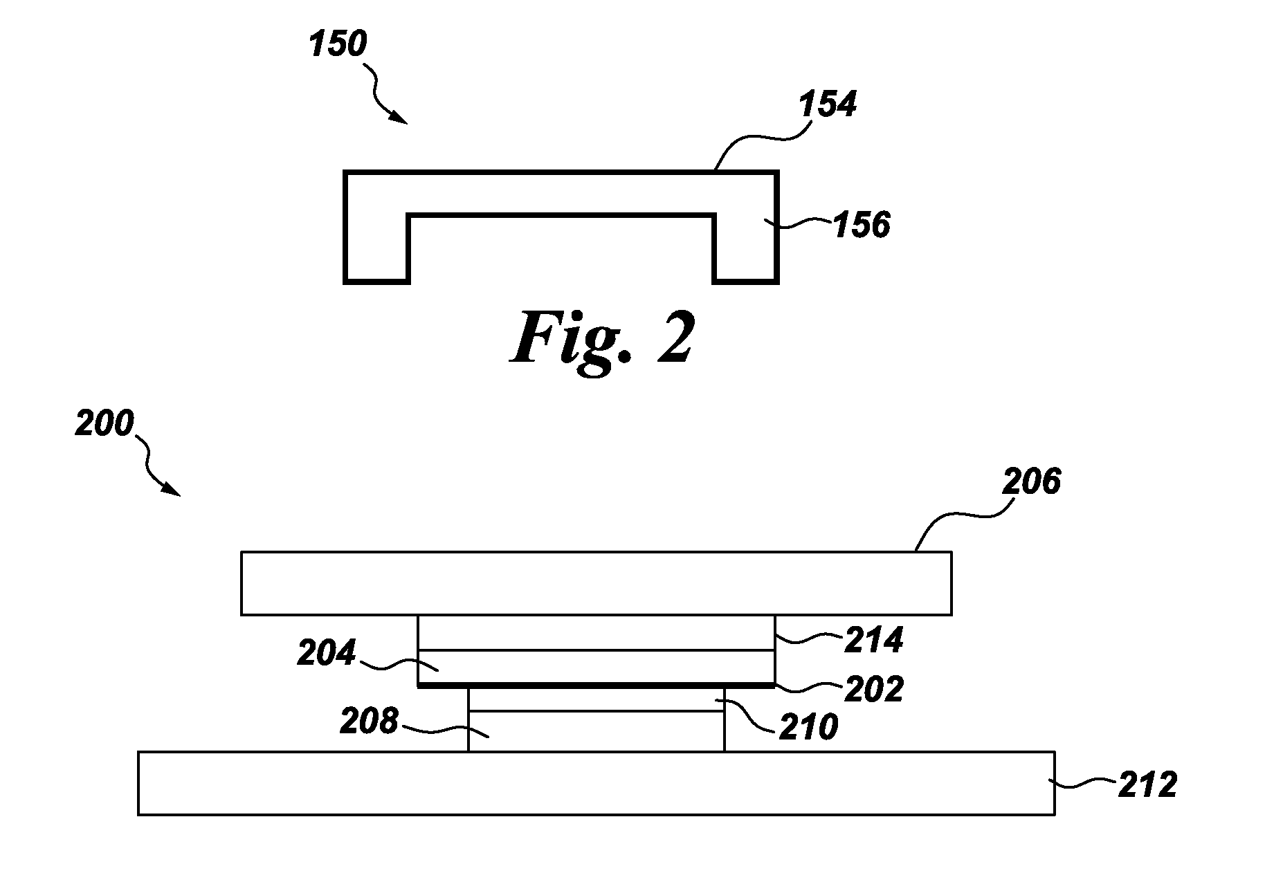
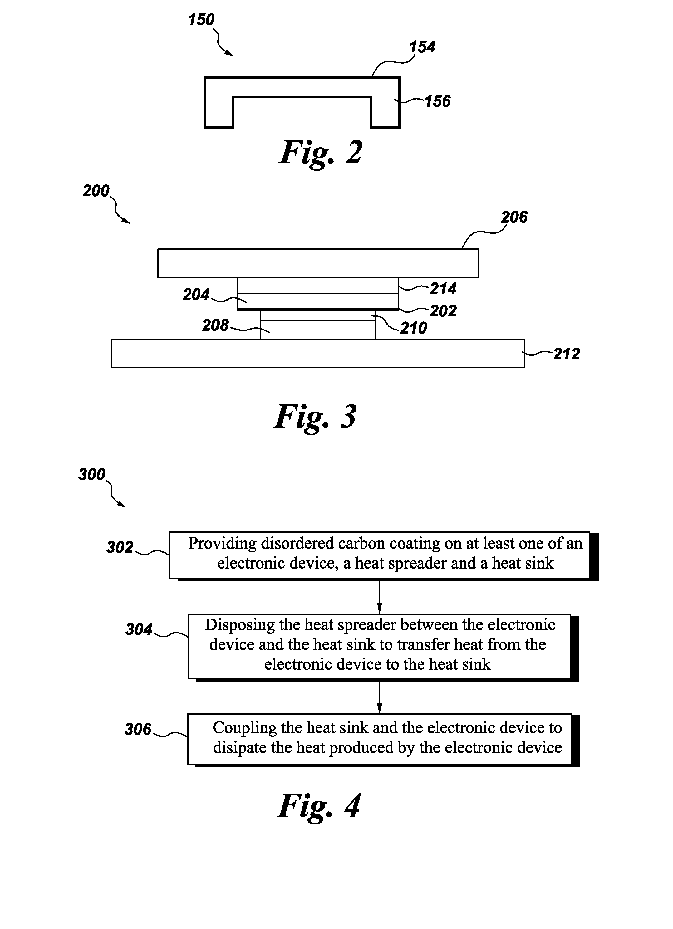
[0013]FIG. 1 illustrates a schematic view of a conventional electronic device assembly 100. In the illustrated embodiment, an electronic device such as a silicon chip 102 (also called as integrated chip) is shown. However, in other embodiments, the electronic device may be any other circuit component or a plurality of circuit components such as semiconductor switching devices, resistors and capacitors. Furthermore, in FIG. 1, only one silicon chip 102 is shown for ease of explanation, although the silicon chip 102 may be part of a larger circuit (not shown). The silicon chip 102 is mounted on a substrate 104 which is further mounted on a printed circuit board (PCB) 106.

[0014]The silicon chip 102 produces heat when energized and / or in operation. A heat sink 108 is coupled to the silicon chip 102 to dissipate the heat generated by the silicon chip into the surrounding medium. The heat sink 108 may be made from materials such as aluminum or copper alloys which have high thermal conduct...


PUM

PropertyMeasurementUnit
Electrical conductoraaaaaaaaaa
Contentaaaaaaaaaa
Thermal propertiesaaaaaaaaaa

Abstract

An electronic device assembly includes a heat sink coupled to an electronic device to dissipate the heat produced by the electronic device. A heat spreader is coupled between the electronic device and the heat sink to transfer heat from the electronic device to the heat sink. Furthermore, at least one of the electronic device, the heat spreader, and the heat sink is disposed with a disordered carbon coating.

Description

[0001]The present application claims priority to U.S. provisional patent application Ser. No. 62 / 025,231 filed Jul. 16, 2014, incorporated herein by reference in its entirety.BACKGROUND[0002]Embodiments of the present specification relate to thermal interfaces, and more particularly to thermal interface device.[0003]Electronic devices often produce heat during operation that needs to be dissipated away from the electronic devices to prevent over heating of one or more components of the electronic devices. As will be appreciated, overheating of the components of the electronic devices may result in reduced reliability and / or failure of the electronic devices. Heat sinks are often used for dissipating heat away from the electronic devices. A heat sink is a passive component that is used to lower a temperature of an electronic device by dissipating heat away from the electronic device into the surrounding environment. In order for the heat sink to operate efficiently, the heat from the...

Claims


Application Information

Patent Timeline
IPC IPC(8): H05K7/20B23P15/26
CPCB23P15/26H05K7/20427H01L23/3675H01L23/3732H01L23/42H01L2224/16225H01L2224/73253H01L2924/15311H01L2924/16152
Inventor CHAUHAN, SHAKTI SINGHJOHNSON, JAMES NEILHODEN, BRIAN PATRICKKIRK, GRAHAM CHARLES
Owner GENERAL ELECTRIC CO
Why Eureka
Try Eureka