Organic electroluminescence element and lighting device using same

a technology of electroluminescence elements and lighting devices, applied in the direction of solid-state devices, semiconductor devices, thermoelectric devices, etc., can solve the problems of reducing the efficiency of light propagation to the outside in which light emission is observed, and 70 to 80 % of the total amount of produced light does not effectively contribute to light emission, etc., to achieve enhanced light-outcoupling efficiency, reduced view angle dependence, and increased efficiency of light emerging outside

Active Publication Date: 2016-02-04
PANASONIC CORP
View PDF2 Cites 12 Cited by
  • Summary
  • Abstract
  • Description
  • Claims
  • Application Information

AI Technical Summary

Benefits of technology

[0032]Due to the present invention, an optical interference in view of plasmon loss is used and therefore an amount of light emerging outside can be increased efficiently. As a result, it is possible to obtain the organic EL element and the lighting device which have the enhanced light-outcoupling efficiency and the reduced view angle dependence, and thereby are excellent in the light emitting property.

Problems solved by technology

Such low light-outcoupling efficiency means that 70% to 80% of the total amount of produced light does not effectively contribute to light emission.
This is because, due to total reflection at interfaces between materials with different refractive indexes, light absorption by materials, and the like, light cannot be effectively propagated to an outside in which light emission is observed.

Method used


Image

  • Organic electroluminescence element and lighting device using same
  • Organic electroluminescence element and lighting device using same
  • Organic electroluminescence element and lighting device using same

Examples


second embodiment

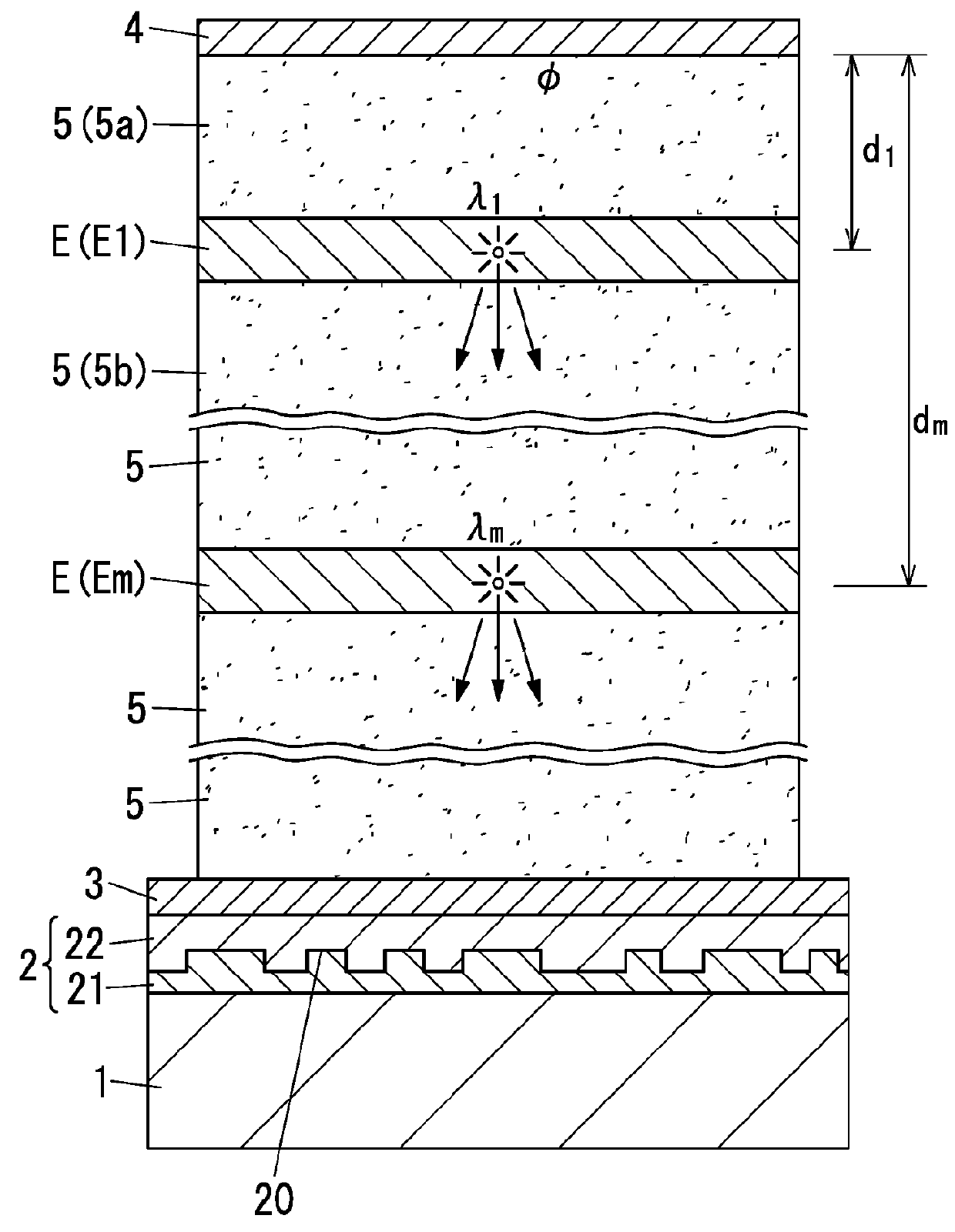
[0060]The present invention is explained with reference to the second embodiment whose reference signs relating to light emitting layers E are expressed by use of general expressions. Note that, the following explanation may be also applied to each embodiment.

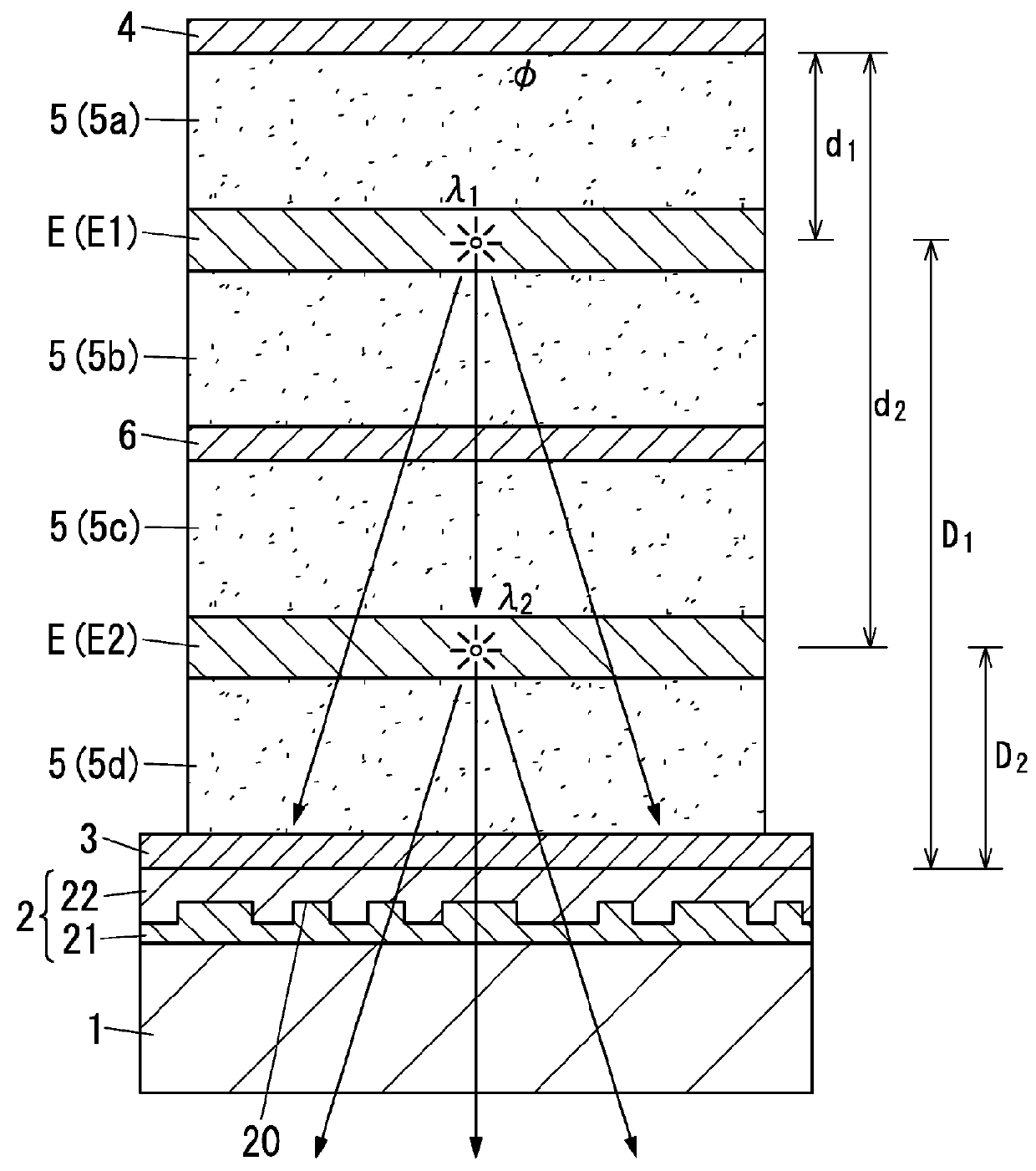
[0061]In the present description, the light emitting layers E includes the m-th closest light emitting layer E to the light reflective electrode 4, which is referred to as an m-th light emitting layer Em. In this regard, m is an integer equal to or more than 1. For example, the first closest light emitting layer E to the light reflective electrode 4 is referred to as a first light emitting layer E1. Additionally, the second closest light emitting layer E to the light reflective electrode 4 is referred to as a second light emitting layer E2.

[0062]λm represents a weighted average emission wavelength of the m-th light emitting layer Em. For example, a weighted average emission wavelength of the first light emitting layer E1 is rep...

third embodiment

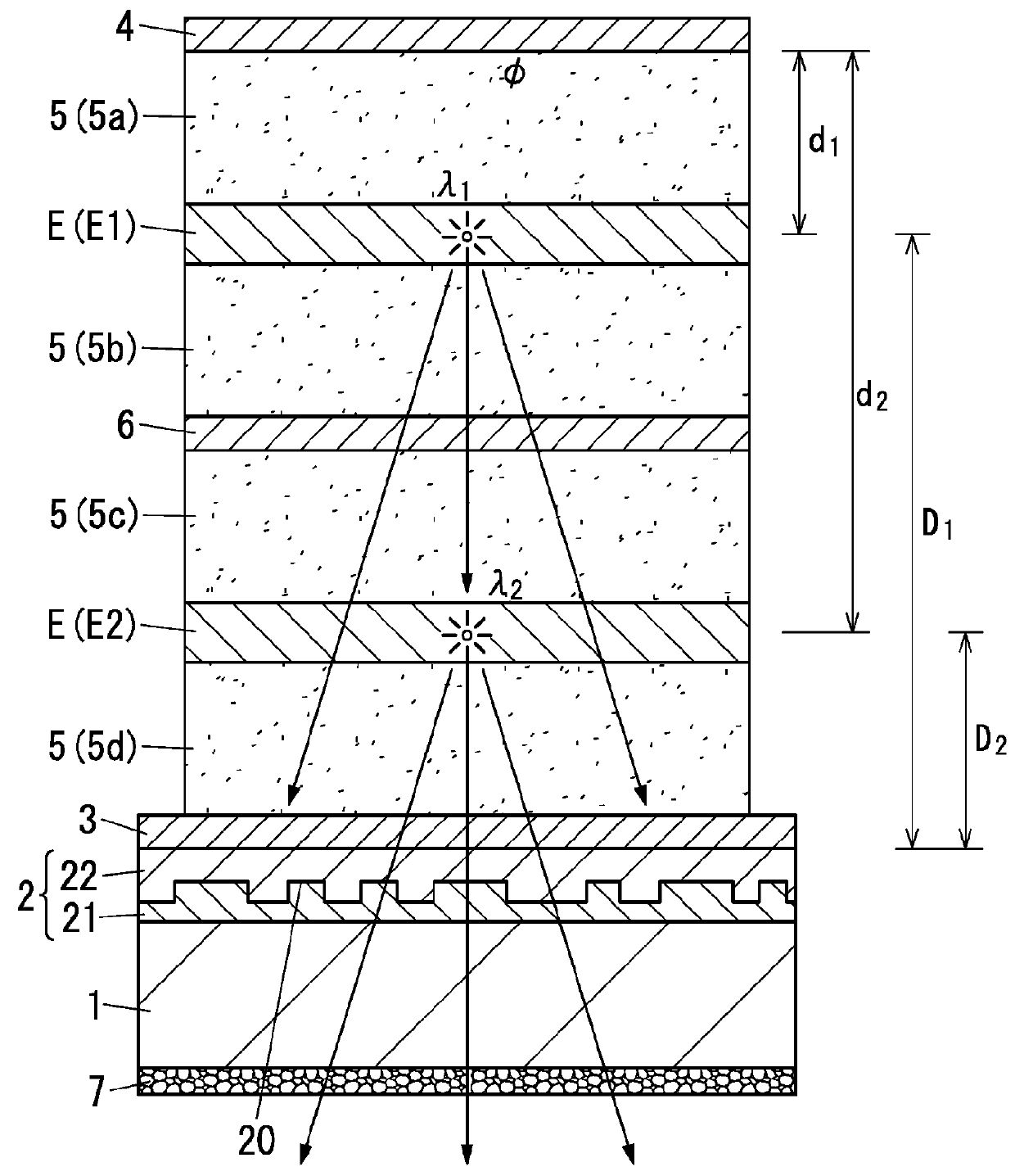
[0085]In the third embodiment, the light-outcoupling layer 7 is provided to the opposite surface of the substrate 1 from the light diffusion layer 2. When the light-outcoupling layer 7 is provided, total reflection at an interface between the substrate 1 and an outside (atmosphere) can be suppressed, and an amount of light emerging outside can be increased.

[0086]Note that, a distance from the light emitting layer E to a surface of the light transmissive electrode 3 facing the substrate 1 is represented by D. The reference point of the position of the light emitting layer E for determining the distance D may be same as that for determining the distance d, and may be the center of the light emitting layer E in the thickness direction thereof.

[Design of Element]

[0087]With reference to a design model of the organic EL element, it is explained that the aforementioned relations are preferable.

[0088]FIG. 4 shows the design model of the organic EL element. This design model is used to optim...

first embodiment

[0098]First, the organic EL element with the multi-unit structure was prepared, experimentally. This prototype has the same layer structure as the first embodiment illustrated in FIG. 1. The whole emission color of this is white. The white emission is important for the lighting use and the like. The first light emitting layer E1 has the weighted average emission wavelength (λ1) of 600 nm. The emission color of the first light emitting layer E1 is orange. The second light emitting layer E2 has the weighted average emission wavelength (λ2) of 470 nm. The emission color of the second light emitting layer E2 is blue. The medium filling the space between the first light emitting layer E1 and the light reflective electrode 4 has the average refractive index (n) of 1.80, and the extinction coefficient (k) of 0.0005. These refractive index and extinction coefficient are averages with regard to the wavelength λ1. The medium filling the space between the second light emitting layer E2 and the...


PUM

PropertyMeasurementUnit
diameteraaaaaaaaaa
refractive indexaaaaaaaaaa

Abstract

The present disclosure relates to an organic electroluminescence element including: a substrate having a light transmissive property; a light diffusion layer; a light transmissive electrode; a light reflective electrode; and multiple light emitting layers spaced from each other. With regard to the m-th light emitting layer being the m-th closest light emitting layer to the light reflective electrode, relations defined by following expressions (2) and (3) are satisfied. In the following expressions, λm represents the weighted average emission wavelength, Ø(λm) represents the phase shift, nm(λm) represents the average refractive index of a medium filling a space between the light reflective electrode and the m-th light emitting layer, and dm represents the distance from the light reflective electrode to the m-th light emitting layer. 1 is an integer equal to or more than 0.φ(λm)×λm4π+l+0.12λm≤nm(λm)×dm≤φ(λm)×λm4π+l+0.62λm(2)nm(λm)×dm≥0.6λm(3)

Description

TECHNICAL FIELD[0001]The present invention relates to organic electroluminescence elements, and lighting devices using same, and in particular relates to an organic electroluminescence element including multiple light emitting layers, and a lighting device.BACKGROUND ART[0002]In a generally known structure of an organic electroluminescence element (hereinafter referred to as “organic EL element”), an anode made of a transparent electrode, a hole transport layer, a light emitting layer, an electron injection layer, and a cathode are stacked on a surface of a transparent substrate in this order. In this organic EL element, light is produced in an organic light emitting layer in response to application of voltage between the anode and the cathode, and the produced light passes through the transparent electrode and the transparent substrate and emerges outside.[0003]Generally, the organic EL element has the light-outcoupling efficiency in the range of about 20% to 30%. Such low light-ou...

Claims


Application Information

Patent Timeline
Patent Type & Authority Applications(United States)
IPC IPC(8): H01L51/50H01L51/52
CPCH01L51/504H01L51/506H01L51/5262H01L51/5206H01L51/5281H01L51/5221H10K85/791H10K50/11H10K2101/40H10K50/131H10K50/854H10K50/19H10K50/856H10K50/13H10K50/81H10K50/82H10K50/85H10K50/86H10K50/155
Inventor YAMAE, KAZUYUKIIDE, NOBUHIROTAKANO, HITOMICHI
Owner PANASONIC CORP
Why Eureka
Try Eureka