Method for manufacturing conductive pattern and conductive pattern formed substrate

a technology of conductive pattern and substrate, which is applied in the direction of conductive pattern formation, dielectric characteristics, instruments, etc., can solve the problem of large number of steps and achieve the effect of simple steps

Active Publication Date: 2016-03-10
RESONAC CORP
View PDF25 Cites 15 Cited by
  • Summary
  • Abstract
  • Description
  • Claims
  • Application Information

AI Technical Summary

Benefits of technology

[0033]According to the present disclosure, a narrow-...

Problems solved by technology

Accordingly, the photolithography has drawbacks that a large...

Method used


Image

  • Method for manufacturing conductive pattern and conductive pattern formed substrate
  • Method for manufacturing conductive pattern and conductive pattern formed substrate
  • Method for manufacturing conductive pattern and conductive pattern formed substrate

Examples


example 1

[0076]SLV-NW-35 (isopropanol dispersion liquid, silver nanowire having a diameter of 35 nm and a length of approximately 15 μm (catalog value), manufactured by Blue Nano, Inc.) was used as a silver nanowire dispersion liquid. A small amount of terpineol (manufactured by Nippon Terpene Chemicals Inc.) was added to this silver nanowire dispersion liquid, and dispersed well. Thereafter, isopropanol was distilled away, and solvent displacement was performed. Then, Tersorb MTPH (isobornyl cyclohexanol, manufactured by Nippon Terpene Chemicals, Inc.) and terpineol were added so that the final concentration of the dispersion medium became terpineol / Tersorb MTPH=1 / 8 (mass ratio), and were dispersed well using ARV-310 manufactured by Thinky Corporation to thereby obtain dispersion liquid. The small amount of terpineol which was added first was predetermined by calculation so that the concentration of the finally obtained dispersion liquid has a silver nanowire concentration of 1% by mass.

[00...

example 2

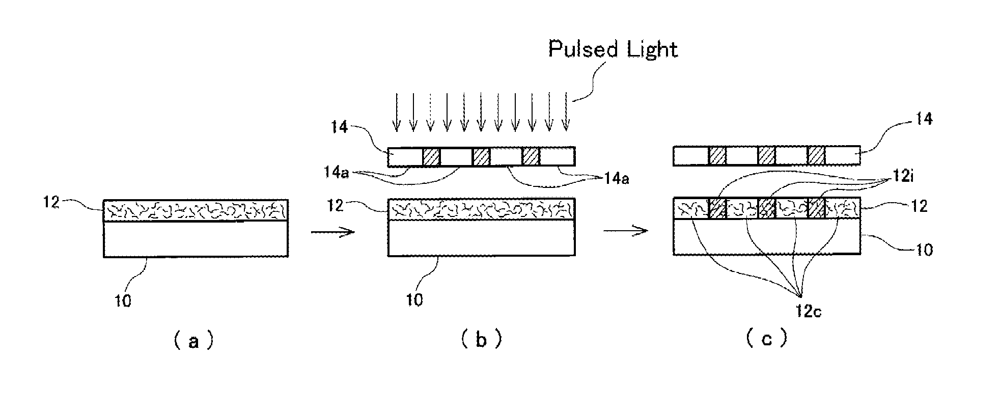
[0082]An ink was prepared by adding poly-N-vinylpyrrolidone (hereinbelow, referred to as PNVP, K-90, molecular weight: 360,000, manufactured by Nippon Shokubai Co., Ltd.) to the ink produced in Example 1, so that the resulting ink containing 0.5 parts by mass of poly-N-vinylpyrrolidone relative to the 99.5 parts by mass of silver nanowire. Using the thus produced ink, an 11-cm-square metal nanowire layer 12 was printed on LUMIRROR (registered trademark) (biaxially oriented polyester film, thickness: 125 μm, manufactured by Toray Industries, Inc.), by a screen printer MT-320 TVZ (manufactured by Microtek Inc.). The thickness of the metal nanowire layer 12 after being dried was 0.15 μm.

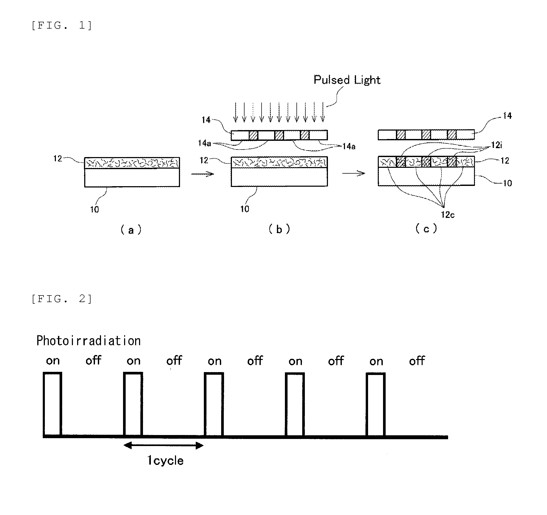
[0083]Next, a mask 14 provided with a light transmission portion 14a in a pattern shown in FIG. 5 was prepared and aligned with the above-mentioned 11-cm-square metal nanowire layer 12, which was subjected to pulsed light irradiation (irradiation energy: 1.0 J / cm2) performed at an irradiation voltage of...

example 3

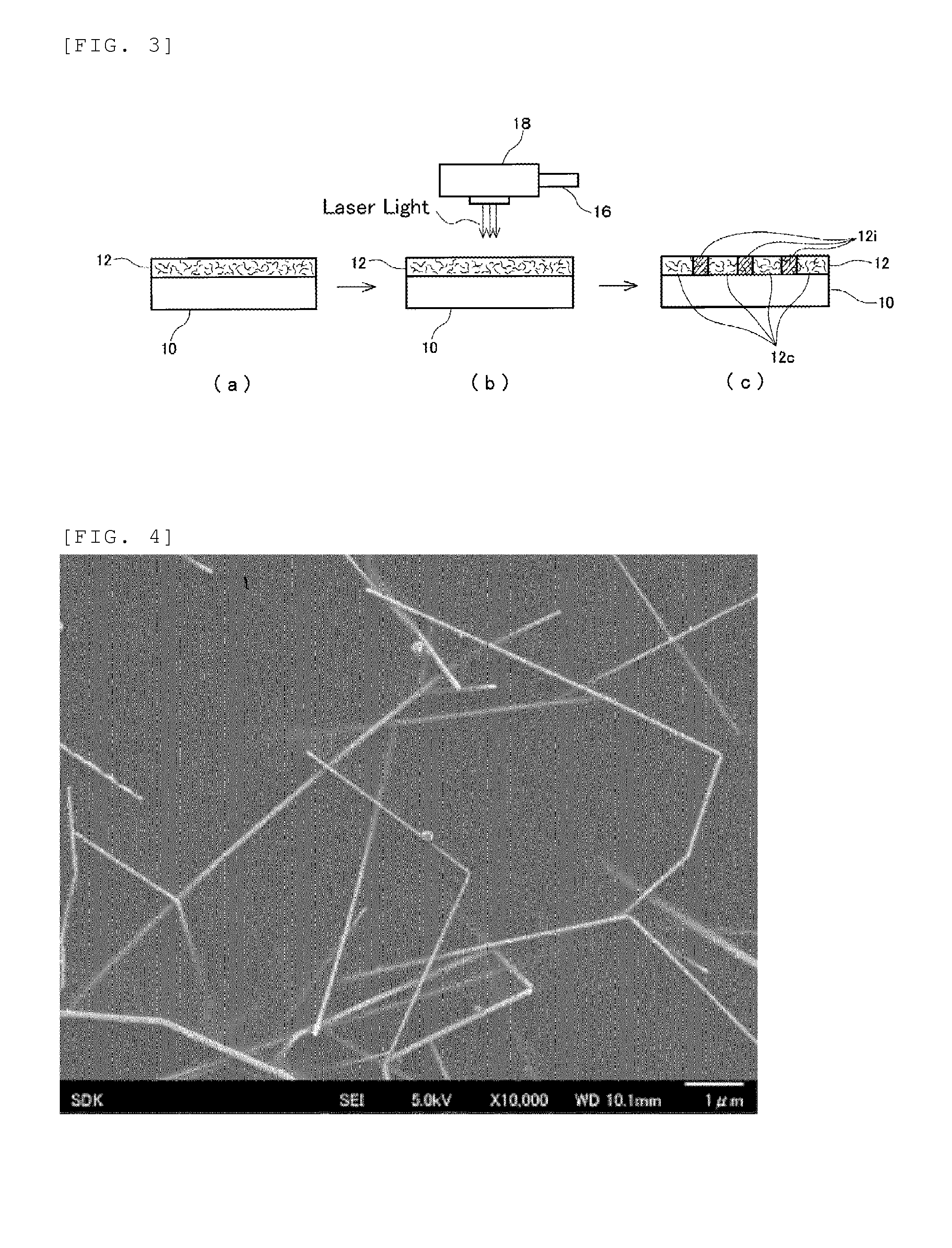
[0087]1 g of poly-N-vinylpyrrolidone (hereinbelow, referred to as PNVP, K-90, molecular weight: 360,000, manufactured by Nippon Shokubai Co., Ltd.) as a binder resin was dissolved in 9 g of terpineol to prepare a PNVP 10% by mass terpineol solution. 250 mg of a silver nanowire 2% by mass terpineol dispersion liquid, the silver nanowire dispersion liquid being prepared by solvent displacement as in Example 1 while the quantitative ratios were changed, 350 mg of terpineol, and 1 g of methyl isobutyl ketone (hereinbelow, referred to as MIBK, manufactured by Tokyo Chemical Industry, Co., Ltd.) were added to 400 mg of this PNVP terpineol solution. The resulting solution was subjected to shaking and stirring for one minute at a room temperature of 25° C., by VORTEX3, a new vortex shaker suitable for short-time operation (manufactured by IKA Corp.). Thereby, an ink was prepared.

[0088]The ink prepared by the above method was coated on a substrate made of a 100-μm-thick PET film (KFL10W, man...


PUM


Abstract

Provided are a conductive pattern manufacturing method and a conductive pattern formed substrate, capable of easily achieving a narrow pitch. A metal nanowire layer 12 is formed on the entirety of a part of at least one of the main faces of a substrate 10, pulsed light is irradiated thereto through a mask 14 provided with a light transmission portion 14a formed in a predetermined pattern, and the metal nanowires in the metal nanowire layer 12 at the region having the above predetermined pattern were sintered, to thereby obtain conductivity at the predetermined patterned region. Accordingly, a substrate provided with a conductive pattern having any selected pattern can be produced by simple steps.

Description

TECHNICAL FIELD [0001]The present disclosure relates to a method for manufacturing a conductive pattern, and a conductive pattern formed substrate.BACKGROUND ART[0002]Recently, various electronic devices such as a mobile phone, a mobile terminal, a personal computer, or the like, are provided with a display panel on which an optically transparent touch panel is attached. Such an electronic device can receive an instruction operation when a user operates on the surface of the touch panel with his / her finger, etc., while the user visually recognizes the display on the display panel through the touch panel.[0003]As for such a touch panel, for example, an electrostatic capacitance touch panel is known, which has a transparent substrate on which a predetermined shaped transparent electrode pattern is formed in the X-direction, and similar transparent electrode pattern is formed in the Y-direction (the direction perpendicular to the X-direction).[0004]A transparent electrode pattern used ...

Claims


Application Information

Patent Timeline
IPC IPC(8): G06F3/041H05K1/02H05K1/09H05K3/10H05K3/12
CPCH05K1/0274H05K1/097H05K3/105G06F2203/04103H05K3/1216H05K3/1283H05K2201/0108G06F3/041H10K71/60H01L21/02603H01L21/0274H01L29/0669H01L29/413
Inventor UCHIDA, HIROSHISHINOZAKI, KENJIOKAZAKI, ERIOHATA, HIDEKIMIYAMURA, YASUNAO
Owner RESONAC CORP
Why Eureka
Try Eureka