
Multilayer ceramic capacitor

a ceramic capacitor and multi-layer technology, applied in the direction of fixed capacitor details, fixed capacitors, printed circuit non-printed electric components association, etc., can solve the problems of degrading the resistance to moisture and damage to the external electrode, and achieve the effect of improving the thermal conductivity (heat release performance) of the base layer, increasing the laser resistance of the external electrode, and high cu content ra

Active Publication Date: 2016-03-31
MURATA MFG CO LTD
View PDF13 Cites 23 Cited by
  • Summary
  • Abstract
  • Description
  • Claims
  • Application Information

AI Technical Summary

Benefits of technology

The present invention is about a multilayer ceramic capacitor with an external electrode that has excellent laser resistance and moisture resistance. The invention provides a solution to improve the thermal conductivity and laser resistance of the external electrode by increasing the content rate of copper in the base layer and reducing the difference in level between the surface of a multilayer printed wiring board and the external electrode surface. The invention also improves the mechanical strength of the component by narrowing the gap between the multilayer printed wiring board and the external electrode and reducing peeling. The invention uses a plating solution with high glass erosion capability to efficiently dissolve the glass in the base layer and penetrate the copper metal into the base layer, resulting in an increased copper content rate and improved thermal conductivity. Additionally, the glass composition of the base layer is optimized to reliably dissolve the glass and prevent peeling between the multilayer printed wiring board and the external electrode.

Problems solved by technology

This is because the external electrodes may be damaged unless the electrodes have laser resistance.
Therefore, peeling is likely to be caused between the multilayer printed wiring board and the external electrodes, and there is also a problem of moisture ingress from the peeled sites, which results in degraded resistance to moisture.

Method used


Image

  • Multilayer ceramic capacitor
  • Multilayer ceramic capacitor
  • Multilayer ceramic capacitor

Examples


experimental examples

1. Preparation of Evaluation Sample

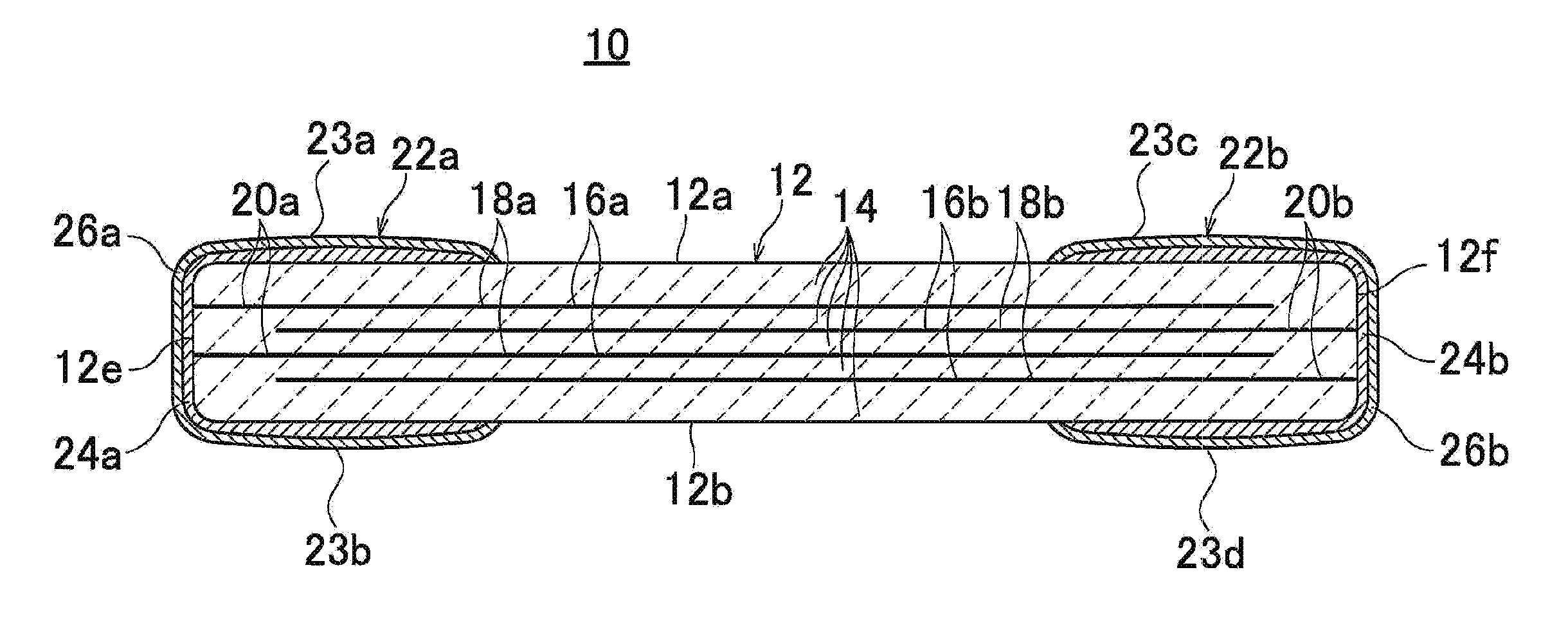
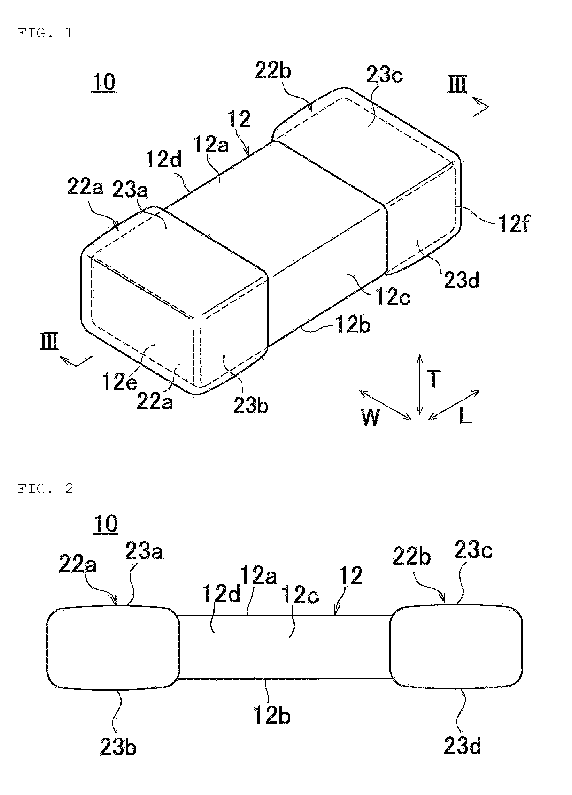
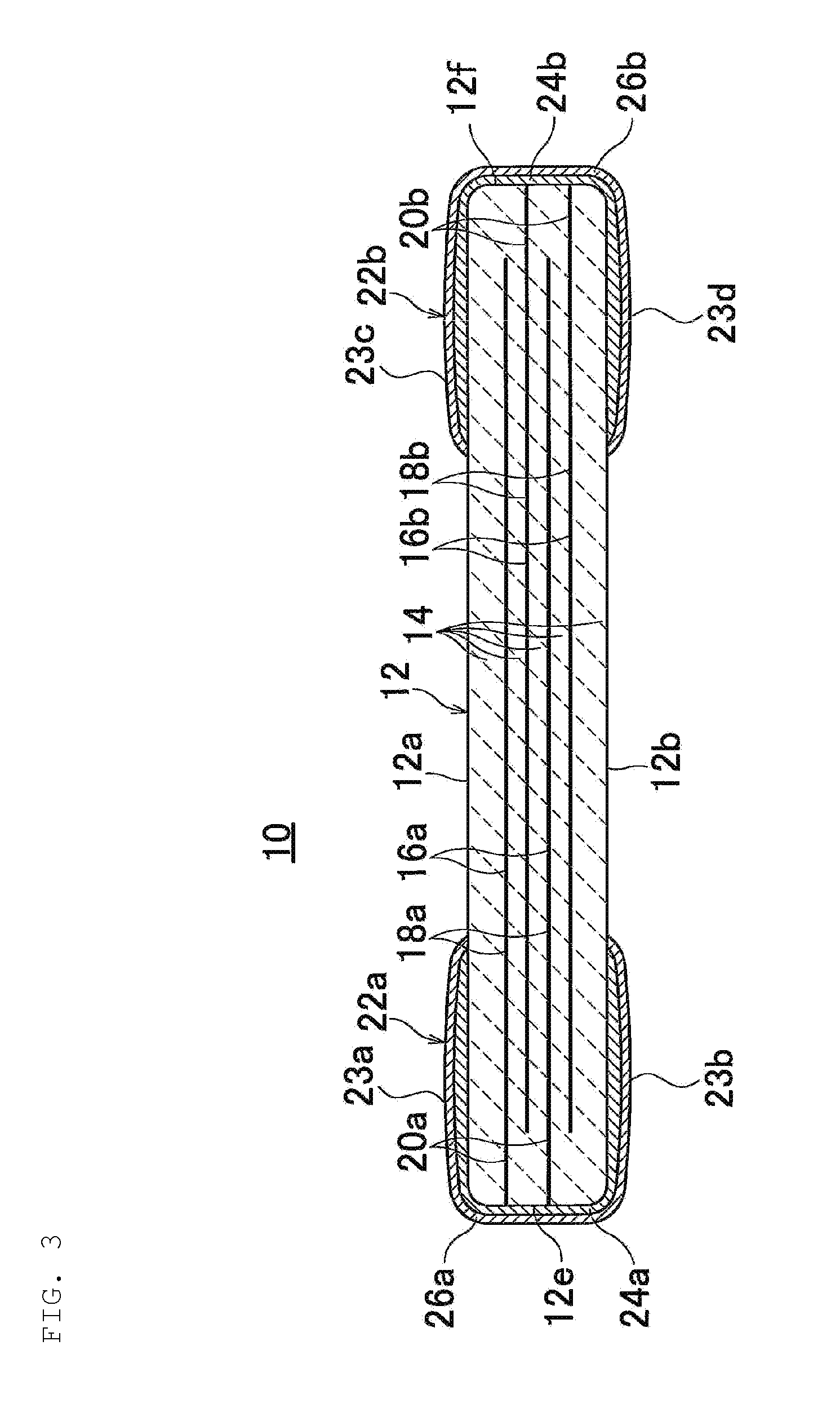
[0166]In the experimental examples, in order to evaluate the external electrodes 22a, 22b for laser resistance and moisture resistance, evaluation samples of the multilayer ceramic capacitor 10 according to Examples 1 to 3 and Comparative Examples 1 to 6 were prepared by controlling the Cu metal of the plated layers 26a, 26b respectively to penetrate into the base layers 24a, 24b, without control for achieving desired arithmetic mean roughness (Ra) of the ceramic body 12 in the step S3 of the manufacturing method mentioned in the previously described preferred embodiment, control for achieving desired arithmetic mean roughness (Ra) of the external electrodes 22a, 22b in the step S7 thereof, and controlling for reducing the impurities in the step S8. The plated layers 26a, 26b are entirely composed of Cu plating. In the formation of the Cu plated layers 26a, 26b, a pyrophosphoric acid Cu plating solution at pH 8.0 was used in the case of Examples 1 ...


PUM

PropertyMeasurementUnit
Lengthaaaaaaaaaa
Lengthaaaaaaaaaa
Lengthaaaaaaaaaa

Abstract

A multilayer ceramic capacitor includes an external electrode on an end surface of a ceramic body to be connected to internal electrodes including a base layer including a sintered metal containing Cu and glass and a Cu plated layer on the base layer. The external electrode includes a principal surface portion disposed on a principal surface of the ceramic body. The Cu metal of the Cu plated layer is present in the base layer to a position of about ⅓ or more of the thickness of the base layer from a surface layer of the external electrode. The metal thickness of the external electrode is about 8.7 μm or more and about 13.9 μm or less.

Description

BACKGROUND OF THE INVENTION[0001]1. Field of the Invention[0002]The present invention relates to a multilayer ceramic capacitor.[0003]2. Description of the Related Art[0004]In recent years, with the reduction in size and height for electronic devices such as cellular phones and portable music players, multilayer printed wiring boards mounted on the electronic devices have been progressively reduced in size. Accordingly, multilayer ceramic capacitors mounted on the multilayer printed wiring boards have been also progressively reduced in size and height.[0005]Some of the multilayer ceramic capacitors are built into multilayer printed wiring boards, such as the multilayer ceramic capacitor described in, for example, Japanese Patent Application Laid-Open No. 2002-203735. In the case of building the multilayer ceramic capacitor into Japanese Patent Application Laid-Open No. 2002-203735, there is a need to irradiate external electrodes of the multilayer ceramic capacitor with a laser to f...

Claims


Application Information

Patent Timeline
IPC IPC(8): H05K1/18H01G4/012H01G4/12H01G4/224H01G4/30H05K1/02H05K1/11
CPCH05K1/183H01G4/30H01G4/224H05K2201/10015H01G4/12H05K1/0298H05K1/115H01G4/012H05K1/0271H05K1/181H01G4/2325
Inventor YOSHIDA, AKIHIRO
Owner MURATA MFG CO LTD
Learn More