
Silicon single crystal growing device and method of growing the same

a single crystal and growing device technology, applied in the direction of crystal growth process polycrystalline material growth, etc., can solve the problems of reducing crucible cannot be liquefied in a short time, and the size standard of an apparatus for growing a single crystal becomes greater, so as to reduce the process time required for growing a single crystal and prevent localized solidification of silicon melt. , the effect of easy control of th

Active Publication Date: 2016-04-14
LG SILTRON
View PDF4 Cites 3 Cited by
  • Summary
  • Abstract
  • Description
  • Claims
  • Application Information

AI Technical Summary

Benefits of technology

The patent text describes how to control the temperature and prevent solidification of silicon melt, which can improve the quality and speed of pulling silicon single crystals. The invention also allows for better control of the thermal environment around the interface of the silicon single crystal, which can help to melt poly silicon faster and reduce the time required to grow a single crystal.

Problems solved by technology

However, as the silicon ingot comes to have a larger diameter, the size standard for an apparatus for growing a single crystal becomes greater, and more particularly, when a crucible becomes larger, poly silicon to be melted in the crucible cannot be liquefied in a short time, so that the process time for growing a single crystal becomes longer.
Also, when a solidification of silicon melt is locally generated because the silicon melt itself cannot be maintained at a uniform temperature, there are problems in that a loss is generated in a silicon single crystal which is to be grown, and the quality of the grown single crystal is also affected.
Also, there is a problem in that a loss occurs in a silicon single crystal because a non-uniform temperature distribution occurs at the surface of the melt and inside the melt in a crystal growing process.

Method used


Image

  • Silicon single crystal growing device and method of growing the same
  • Silicon single crystal growing device and method of growing the same
  • Silicon single crystal growing device and method of growing the same

Examples


first embodiment

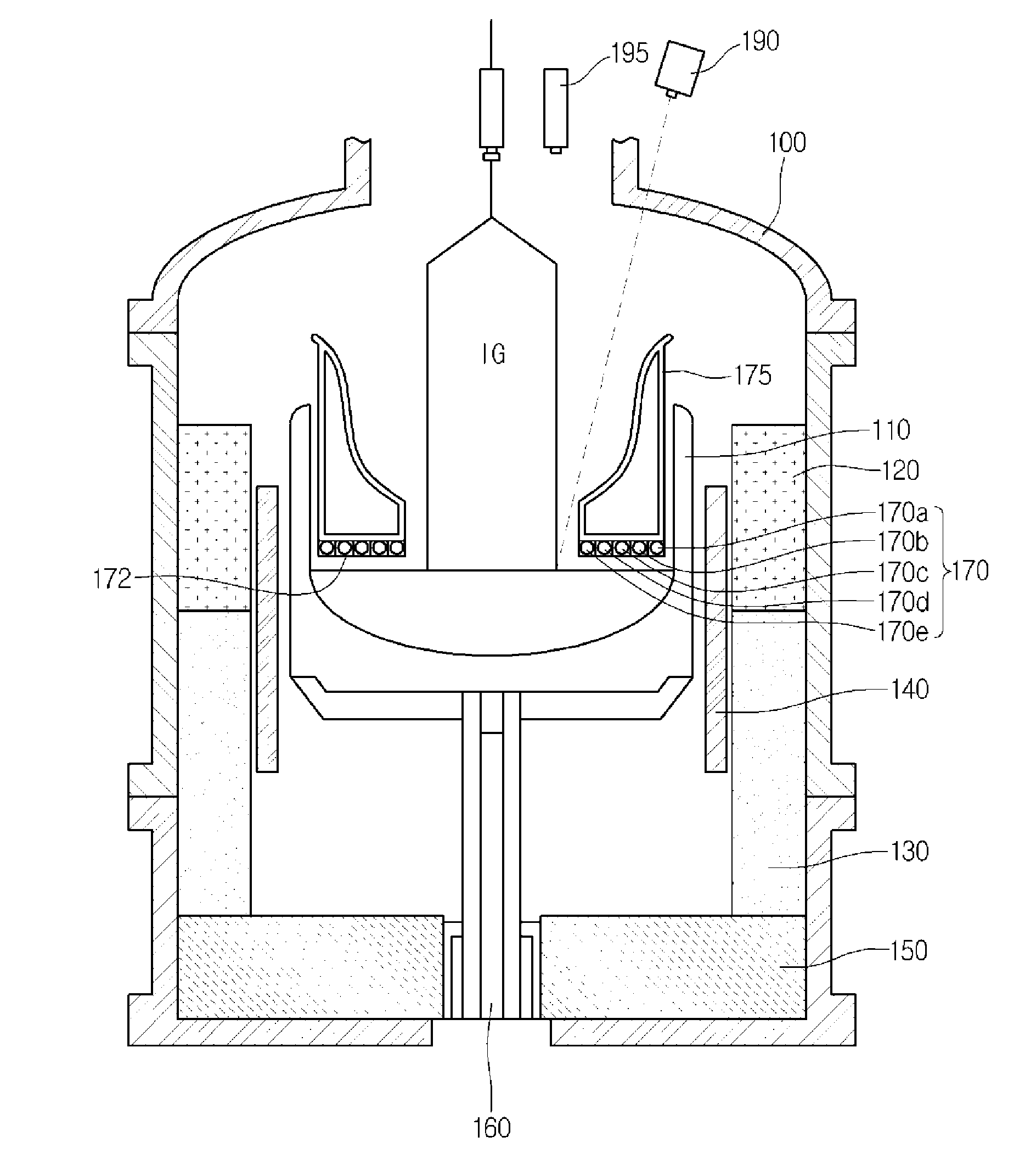
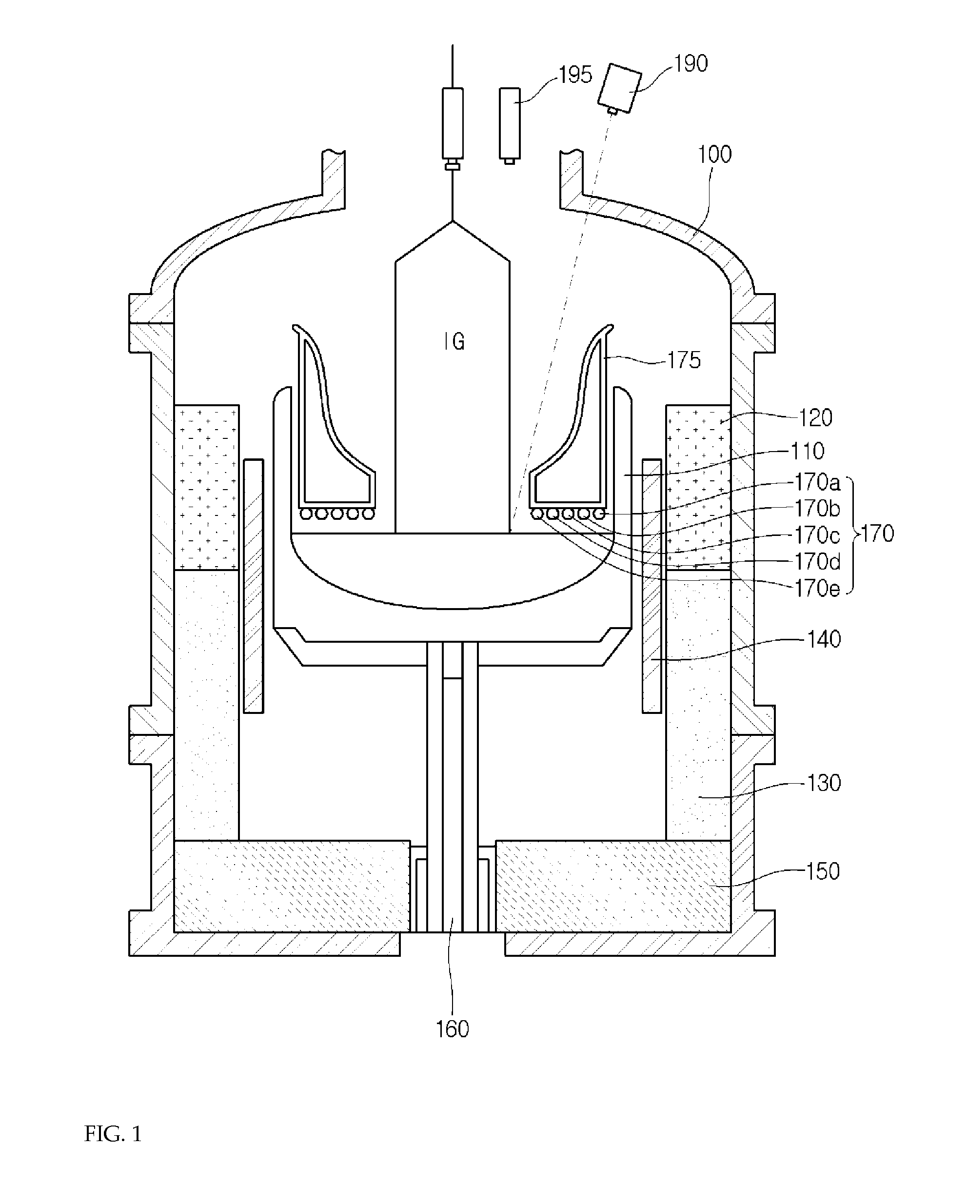
[0020]FIG. 1 is a cross-sectional view illustrating an apparatus for growing a single crystal according to a

[0021]Referring to FIG. 1, as illustrated above, the apparatus for growing a single crystal includes: a chamber 100 including a crucible 110 accommodating silicon melt; a support shaft 160 for rotating and lifting the crucible 110 while supporting the crucible 110; a main heater part 140 disposed beside the crucible 110 to apply heat to the crucible 110 side; a side surface heat insulation member 130 disposed in a side direction of the main heater part 140; a side upper heat insulation member 120 located on the side surface heat insulation member 130; an upper heater part 170 including a plurality of heater parts 170 for generating heat over the silicon melt; and an upper heat insulation member 175 for blocking the heat generated from the heater part 170.

[0022]In preparing a silicon single crystal using the apparatus for growing a single crystal, poly silicon is accommodated i...

second embodiment

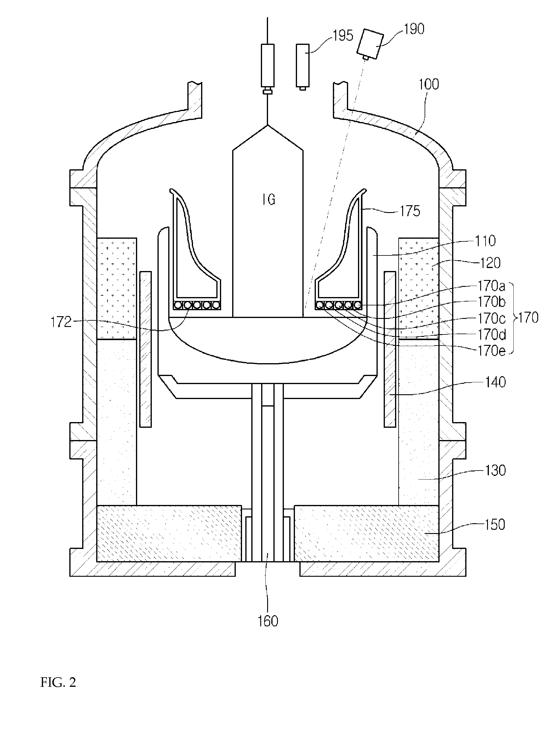
[0032]FIG. 2 is a cross-sectional view illustrating an apparatus for growing a single crystal according to a

[0033]Referring to FIG. 2, the second embodiment is characterized by including a heater shield 172 separating each of the plurality of heaters 170a, 170b, 170c, 170d, and 170e of the upper heater part 170 disposed in the apparatus for growing single crystal of the first embodiment. The heater shield may include a side surface blocking film which blocks a side surface of each heater disposed in the heater part 170, and a lower surface blocking film which blocks a lower surface of each heater.

[0034]The heater shield 172 may be formed of tungsten or graphite, and is installed to prevent interference in the heat history between neighboring heaters when each heater operates. That is, in order to more accurately control the temperature of silicon melt, heat generated in each heater should be transferred to a solid-liquid interface located vertically under each heater with a minimal ...

third embodiment

[0042]FIG. 4 is a view illustrating an apparatus for growing a single crystal according to a

[0043]Referring to FIG. 4, the third embodiment may further include a lower heater part 176 in the apparatus for growing a single crystal of the third embodiment. Also included may be a control unit 180 which connects the lower heater part 176, the main heater part 140, and the upper heater part 170, and a programmable logic controller (PLC) may be used, for example.

[0044]The lower heater part 176 is located under a crucible support member, and may be formed in a ring shape as the upper heater part 170. The lower heater part 176 is installed to control the temperature at the lower portion of the silicon melt, and may be turned on / off according to the controlling by the control unit. The lower heater part 176 is turned on in a process in which a solid raw material, such as poly silicon, is melted in a crucible, so that the poly silicon may be uniformly melted at upper and lower portions of the...


PUM

PropertyMeasurementUnit
diametersaaaaaaaaaa
temperatureaaaaaaaaaa
melting stateaaaaaaaaaa

Abstract

An apparatus for growing a silicon single crystal according to embodiments includes a chamber including a crucible accommodating silicon melt; a support shaft rotating and lifting the crucible while supporting the crucible; a main heater part for applying heat to the crucible side, the heater disposed beside the crucible; an upper heat insulation member located over the crucible; and upper heater parts located at a lower end portion of the upper heat insulation member, wherein the upper heater parts have diameters different from each other with respect to a center of the crucible, and include a plurality of ring-shaped heaters which are spaced apart from each other. Due to the individually controllable upper heater parts, a uniform thermal environment can be provided for silicon melt accommodated in a crucible, and localized solidification of the silicon melt can be prevented so that the quality of a silicon single crystal and the ingot pulling speed can be readily controlled.

Description

CROSS-REFERENCE TO RELATED APPLICATIONS[0001]The present application is a national phase application of PCT application PCT / KR2014 / 005003 filed Jun. 5, 2014, which claims the priority benefit of Korean patent application 10-2013-0071494 filed Jun. 21, 2013, the disclosures of which are incorporated herein by reference.BACKGROUND OF THE INVENTION[0002]1. Technical Field[0003]The present disclosure relates to an apparatus for growing a single crystal and a method for growing a silicon single crystal, and more particularly to an apparatus for growing a single crystal and a method for growing the same, which provide a thermal environment in which silicon melt accommodated in a crucible can be quickly melted inside the crucible.[0004]2. Background Art[0005]In general, silicon single crystals used as substrates for manufacturing semiconductor devices are manufactured by using the Czochralski (Cz) method. In the Cz method, silicon single crystals are introduced into a quartz crucible, and ...

Claims


Application Information

Patent Timeline
Patent Type & Authority Applications(United States)
IPC IPC(8): C30B15/20C30B15/14C30B29/06C30B15/26
CPCC30B15/206C30B29/06C30B15/14C30B15/26C30B15/20
Inventor JEON, SU-IN
Owner LG SILTRON
Learn More